Module substrate and method for manufacturing module substrate

Active Publication Date: 2013-08-29
MURATA MFG CO LTD
View PDF11 Cites 12 Cited by
  • Summary
  • Abstract
  • Description
  • Claims
  • Application Information

AI Technical Summary

Benefits of technology

[0043]With this configuration, before cutting out a plurality of the module substrates from the collective substrate, the resin layer covering the electronic components mounted on at least the one surface of the collective substrate is formed such that the portion of the terminal connection substrate is exposed therefrom. Thus, the insulation between the electronic components mounted on the one surface of the collective substrate is improved. In addition, since the one surface of the base substrate on which the electronic components and the terminal connection substrate are mounted is previously covered with the resin layer when electronic components are mounted on both surfaces of the collective substrate, it is possible to prevent detachment, movement, or other damage of the electronic components and the terminal connection substrate mounted on the one surface of the base substrate due to stress or the forces generated when electronic components are mounted on the other surface of the base substrate.
[0044]According to various preferred embodiments of the present invention, at least the corner of each conductor portion or the columnar terminal connection substrate is chamfered with a flat surface and/or curved surface, and each conductor portion or the columnar terminal connection substrate is connected, at a side surface thereof contacting the chamfered flat surface and/or curved surface, to the one surface of the base substrate. Thus, it is possible to mount an electronic component below each conductor portion or the terminal connection substrate. Therefore, the size of a region in which electronic components can be mounted is increased, and the number of mountable electronic components is increased. In addition, it is possible to reduce the size of the module substrate even when a required number of electronic components are mounted thereon.
[0045]In addition, according to various preferred embodiments of the present invention, the columnar terminal connection substrate whose cross-sectional shape is a T shape is formed, the columnar terminal connection substrate is connected to the one surface of the collective substrate such that the columnar terminal connection substrate is located over the cut-out position, and a plurality of the module substrates are cut out at the cut-out position from the collective substrate. When a plurality

Problems solved by technology

When the region in which electronic components can be mounted is small, the number of mountable electronic components is reduced, the size of the module sub

Method used


Image

  • Module substrate and method for manufacturing module substrate
  • Module substrate and method for manufacturing module substrate
  • Module substrate and method for manufacturing module substrate

Examples


first preferred embodiment

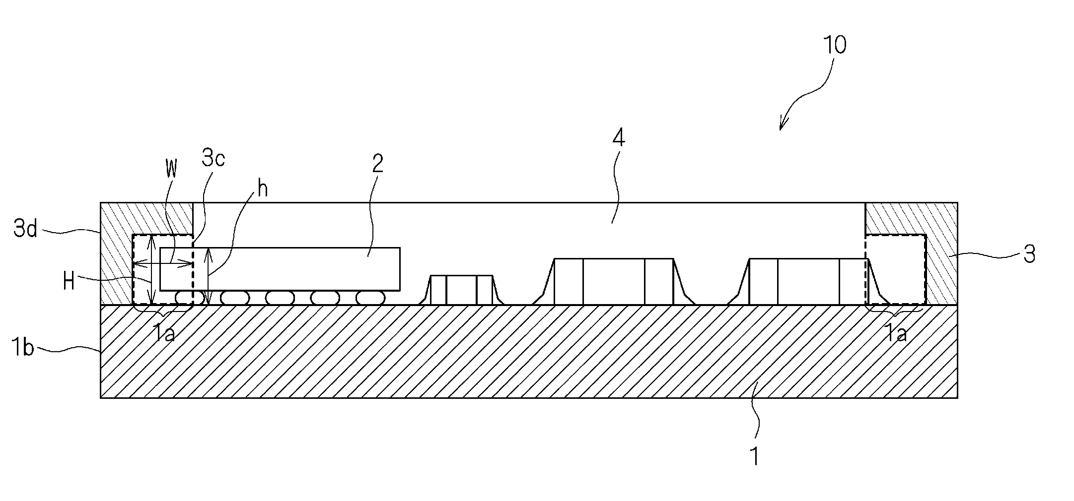
[0067]FIG. 1 is a schematic diagram showing a configuration of a module substrate according to the first preferred embodiment of the present invention. As shown in FIG. 1, the module substrate 10 includes a base substrate 1, a plurality of electronic components 2 mounted on one surface of the base substrate 1, terminal connection substrates 3 connected to the one surface of the base substrate 1 on which a plurality of the electronic components 2 are mounted, and a resin layer 4 covering the electronic components 2 mounted on the one surface of the base substrate 1.

[0068]The base substrate 1 is preferably an LTCC (low temperature co-fired ceramics) substrate, an organic substrate, or other suitable substrate, for example, but is not particularly limited thereto. Surface electrodes (not shown) are provided on the surface of the base substrate 1 on which the electronic components 2 are mounted. The electronic components 2 are surface-mount type electronic components (surface mount devi...

second preferred embodiment

[0093]In a module substrate according to a second preferred embodiment of the present invention, an insulating plate is disposed on a side surface, in an outward direction of a base substrate 1 of a terminal connection substrate 3 connected to one surface of the base substrate 1. FIG. 8 is a schematic diagram showing a configuration of the module substrate according to the second preferred embodiment of the present invention. As shown in FIG. 8, in the module substrate 11, an insulating plate 7 is disposed on a side surface 3d in the outward direction of the base substrate 1 of each terminal connection substrate 3 connected to the one surface of the base substrate 1. It is noted that the module substrate 11 has the same or substantially the same configuration as that of the module substrate 10 shown in FIG. 1, except that the insulating plate 7 is provided, and thus, the same elements are designated at the same reference signs and the detailed description thereof is omitted.

[0094]FI...

third preferred embodiment

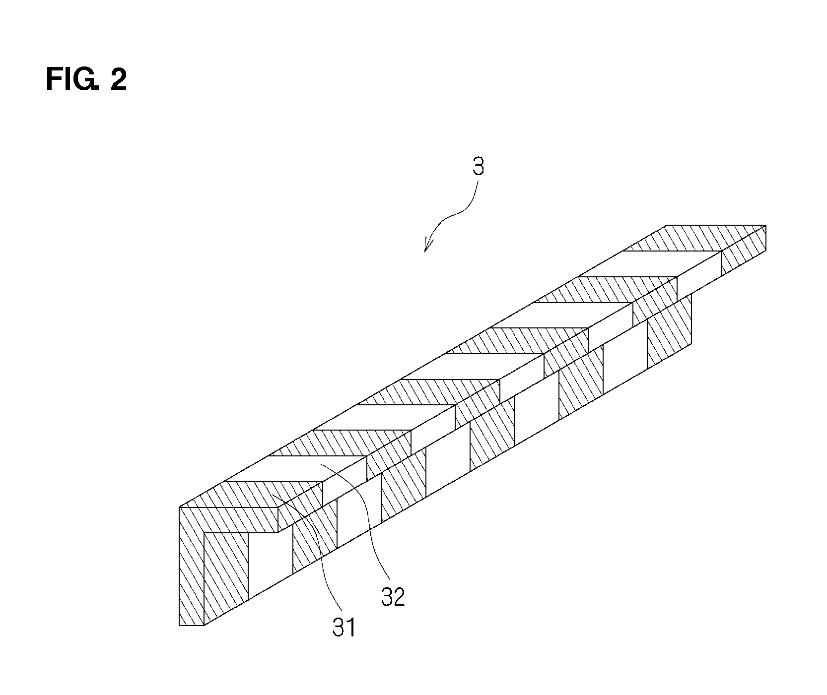
[0103]In a module substrate according to a third preferred embodiment of the present invention, an insulating plate 7 is disposed on a side surface, in an outward direction of a base substrate 1, of a terminal connection substrate 3 connected to one surface of the base substrate 1 similarly to the second preferred embodiment, but the terminal connection substrate 3 does not include an insulating portion. FIG. 12 is a perspective view showing the configuration of the terminal connection substrate 3 according to the third preferred embodiment of the present invention. As shown in FIG. 12, two columnar terminal connection substrates 3 in which a plurality of conductor portions 31 are fixed to each other via an insulating material (support portion) 38 and whose cross-sectional shape is an inverted L shape are provided as one terminal connection substrate 3. In other words, the columnar terminal connection substrate 3 is provided in which the two columnar terminal connection substrates 3...


PUM

PropertyMeasurementUnit
Shapeaaaaaaaaaa
Electrical conductoraaaaaaaaaa

Abstract

A module substrate includes a plurality of electronic components mounted on at least one surface of a base substrate and a columnar terminal connection substrate connected to the one surface of the base substrate on which a plurality of the electronic components are mounted. The terminal connection substrate includes a plurality of conductor portions, at least one corner of the columnar terminal connection substrate is chamfered with a flat surface and/or curved surface, and the terminal connection substrate is connected at a side surface thereof contacting the chamfered surface, to the one surface of the base substrate.

Description

BACKGROUND OF THE INVENTION[0001]1. Field of the Invention[0002]The present invention relates to a module substrate including a terminal connection substrate that is connected to a base substrate including a plurality of electronic components that are mounted on at least one surface thereof, and a method for manufacturing a module substrate.[0003]2. Description of the Related Art[0004]In recent years, with reductions in the size and weight of electronic devices, module substrates mounted in electronic devices have been required to be reduced in size and weight. Thus, a module substrate is reduced in size and weight by mounting electronic components on both surfaces of a base substrate via a lead terminal, a solder ball, a cavity structure, or other suitable structure.[0005]Japanese Unexamined Patent Application Publication No. 2004-303944 discloses a module substrate that includes a main substrate in which a plurality of electronic components are mounted on both surfaces thereof by ...

Claims


Application Information

Patent Timeline
IPC IPC(8): H05K1/02H05K3/28H05K3/30
CPCH01L25/16Y10T29/4913H05K3/0052H05K3/0097H05K3/284H05K2201/1034H05K2201/10477H05K2203/1316H01L23/49811H05K1/0296H05K3/30H01L23/49861H01L23/552H01L24/97H01L2224/16225H01L2224/97H01L2924/15312H01L2924/15322H01L2924/19105H01L2924/19106H05K1/141Y10T29/49146H01L2224/81H01L2924/12042H01L2924/00
Inventor YAMAMOTO, ISSEIOTSUBO, YOSHIHITO
Owner MURATA MFG CO LTD
Why Eureka
Try Eureka