Solid-state device and method of manufacturing the same
Active Publication Date: 2013-09-26
TOYODA GOSEI CO LTD
View PDF6 Cites 17 Cited by
Summary
Abstract
Description
Claims
Application Information
AI Technical Summary
This helps you quickly interpret patents by identifying the three key elements:
Problems solved by technology
Method used
Benefits of technology
Benefits of technology
The invention is about a new type of solid-state device that improves heat dissipation. It does this by creating a cavity in the metal pattern where the conductive bump is formed. This helps to reduce the distance between the substrate and the solid-state element, resulting in better heat dissipation.
Problems solved by technology
Therefore, the LED element is spaced from the substrate by the height of the metal pattern and the conductive bump, which may cause a decrease in heat dissipation.
Method used
Image
Click on the blue label to locate the original text in one second.
Reading with bidirectional positioning of images and text.
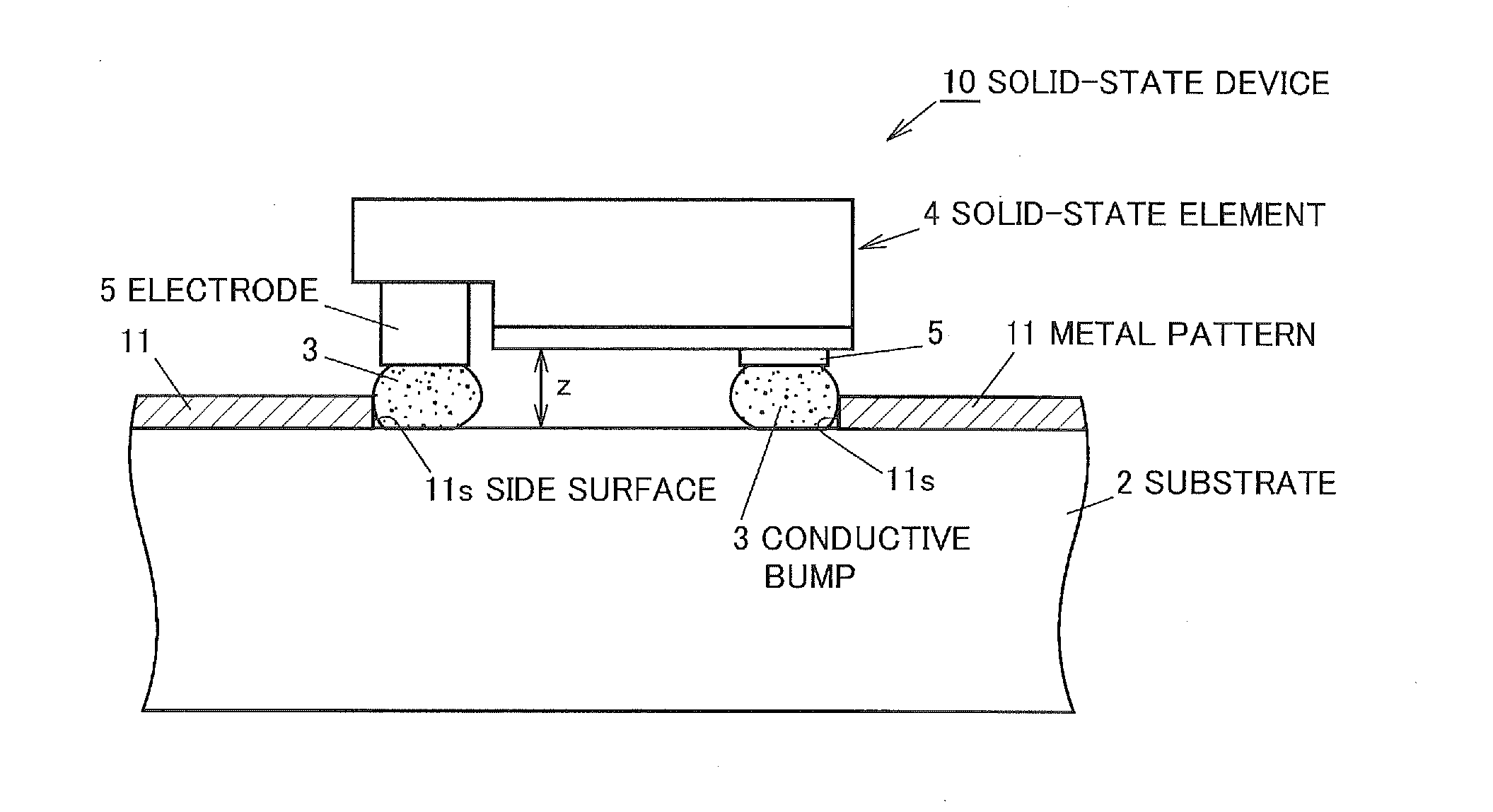
[0049]FIG. 1 is a vertical cross-sectional view showing a portion of a solid-state device in the first embodiment. A solid-state device 10 has a substrate 2, a metal pattern 11 formed on the substrate 2 and a solid-state element 4 connected to the metal pattern 11 via a conductive bump 3.
[0050]The substrate 2 is formed of, e.g., polycrystalline alumina. It is possible to use polycrystalline alumina of which strength is enhanced by adding ZrO or polycrystalline alumina of which reflectance is enhanced by adding light scattering glass. Alternatively the substrate 2 may be formed of a high thermal conductivity member having a thermal conductivity of not less than 100 W / (m·k), such as AlN or Si3N4. In addition, when a process requiring a substrate to have heat resistance, such as hot-melting of low-melting-point glass to seal the solid-state element 4, is not carried out, it is possible to use a low-heat resistant substrate such as glass-epoxy substr...
second embodiment
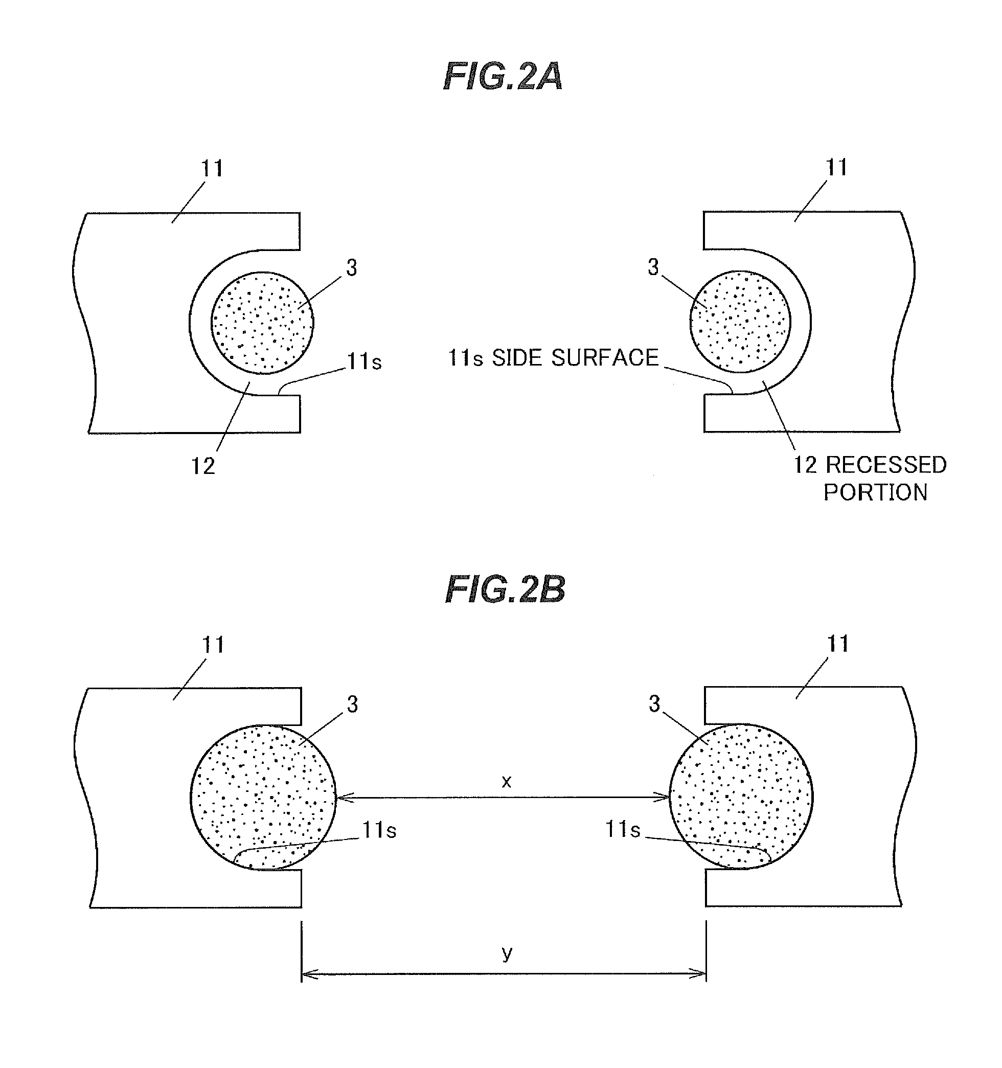
[0069]The second embodiment is different from the first embodiment in the shape of the metal pattern and the position of the conductive bump. Note that, the explanation for the same features as the first embodiment will be omitted or simplified.
[0070]FIG. 7A is a vertical cross-sectional view showing a portion of a solid-state device 20 in the second embodiment FIG. 7B is a top view showing an end portion of a metal pattern 21 and the conductive bump 3 of the solid-state device 20.
[0071]A side surface 21s of the metal pattern 21 is inclined with respect to a vertical direction. When the metal pattern 21 is formed by, e.g., screen-printing and baking Ag paste, inclination is naturally formed after the printing. The Ag paste used for the screen-printing contains Ag particles having a diameter of, e.g., not more than 15 μm, and typically 5±2 μm, The thickness of the metal pattern 21 is, e.g., 10 μm.
[0072]The conductive bump 3 is formed such that a portion of the bottom surface is in co...
third embodiment
[0080]The third embodiment is different from the second embodiment in the shape of the metal pattern and an inclined angle of the side surface. Note that, the explanation for the same features as the second embodiment will be omitted or simplified.
[0081]FIG. 9A is a vertical cross-sectional view showing a portion of a solid-state device 30 in the third embodiment. FIG. 9B is a top view showing an end portion of a metal pattern 31 and the conductive bump 3 of the solid-state device 30.
[0082]The metal pattern 31 has a pointed triangular shape at an end portion to be connected to the solid-state element 4. In addition, a side surface 31s of the metal pattern 31 is inclined with respect to a vertical direction. When the metal pattern 31 is formed by, e.g., screen-printing Ag paste, the inclination of the side surface 31s is shallower than that of the side surface 21s of the metal pattern 21 in the second embodiment since the end portion of the metal pattern 31 has a triangular shape. Th...
PUM
Abstract
A solid-state device includes a metal pattern formed on a substrate, a conductive bump connected to the metal pattern so as to be contact with a side surface of the metal pattern, and a solid-state element connected to the metal pattern via the conductive bump. A bottom surface level of at least a portion of the conductive bump is substantially equal to a bottom surface level of a portion of the metal pattern at which the metal pattern is connected to the conductive bump.
Description
[0001]The present application is based on Japanese patent application Nos.2012-066289 and 2012-275997 filed on Mar. 22, 2012 and Dec. 18, 2012, respectively, the entire contents of which are incorporated herein by reference.BACKGROUND OF THE INVENTION[0002]1. FIELD OF THE INVENTION[0003]The invention relates to a solid-state device and a method of manufacturing the solid-state device.[0004]2. RELATED ART[0005]Conventional solid-state devices include a device that a solid-state element such as LED chip is connected to a metal pattern via a conductive bump (see, e.g., JP-A-2011-222875).SUMMARY OF THE INVENTION[0006]The device disclosed in JP-A-2011-222875 is constructed such that the conductive bump is formed on a connecting terminal as a metal pattern on a substrate and an LED element is formed on the bump. Therefore, the LED element is spaced from the substrate by the height of the metal pattern and the conductive bump, which may cause a decrease in heat dissipation.[0007]Accordingl...
Claims
Application Information
Patent Timeline
Application Date:The date an application was filed.
Publication Date:The date a patent or application was officially published.
First Publication Date:The earliest publication date of a patent with the same application number.
Issue Date:Publication date of the patent grant document.
PCT Entry Date:The Entry date of PCT National Phase.
Estimated Expiry Date:The statutory expiry date of a patent right according to the Patent Law, and it is the longest term of protection that the patent right can achieve without the termination of the patent right due to other reasons(Term extension factor has been taken into account ).
Invalid Date:Actual expiry date is based on effective date or publication date of legal transaction data of invalid patent.

