LED, Backlight Module, and LCD Device

a technology of backlight module and led, which is applied in the field of electromechanical displays, can solve the problems of poor conduction between the chip and the electrode, cracking at the joint of the plastic material and the electrode and the joint, and the chip arrangement of the common led chip does not benefit light dispersal, so as to reduce the oxidation of the electrode and increase the contact area , the effect of strong adaptability

Inactive Publication Date: 2013-10-03
SHENZHEN CHINA STAR OPTOELECTRONICS TECH CO LTD
View PDF5 Cites 55 Cited by
  • Summary
  • Abstract
  • Description
  • Claims
  • Application Information

AI Technical Summary

Benefits of technology

[0018]The invention designs the down set, to increase the contact area between the electrode and the potting adhesive, and reduce electrode oxidation. In addition, the two side walls adjacent to the electrodes of the inner cavity are provided with inclined surface(s); thus, the side light emitted by the chip is directly reflected outside by the inclined surface, thereby expanding the light emitting angel. By selecting the inclination angle of different inclined surfaces, the invention can freely control the scattering range of the emitted light, has strong adaptability, and is suitable for being used as a backlight source of the LCD device. When light enters from the side, the large light emitting angle enables the light to be uniformly emitted into a light guide panel, thereby reducing the phenomenon of hot spots.

Problems solved by technology

These materials have different expansion rate, and thus crack occurs at the joint of the plastic material and the electrode and the joint of the potting adhesive and the electrode.
Thus, the conduction between the chip and the electrode is increasingly poor as time passes by.
All the down set arrangement of the chips of the common LEDs does not benefit light dispersal.

Method used


Image

  • LED, Backlight Module, and LCD Device
  • LED, Backlight Module, and LCD Device
  • LED, Backlight Module, and LCD Device

Examples


example 1

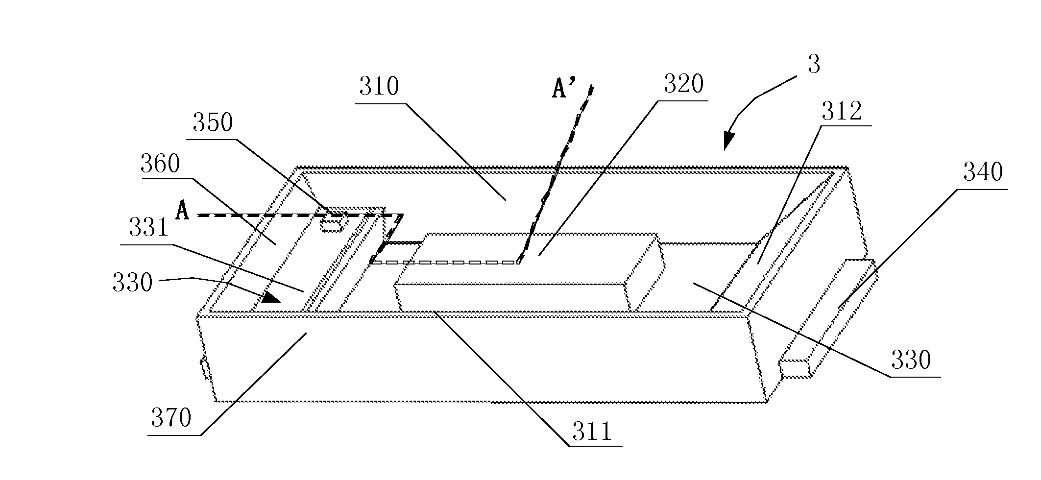
[0032]As shown in FIG. 6, one of the two side walls adjacent to the step surface is provided a first inclined surface 310. The acute angle that the first inclined surface 310 intersects the bottom plane of the inner cavity is between 0.5° and 89°, preferably, between 30° and 60°. The electrodes 330 can be arranged on the two short side walls of the inner cavity, and accordingly, the first inclined surface 310 can be arranged on the long side wall of the inner cavity. Optionally, the electrodes 330 can be arranged on the two long side walls of the inner cavity, and accordingly, the first inclined surface 310 can be arranged on the short side wall of the inner cavity.

[0033]To prevent the chip from being broken down by static electricity, one of the electrodes is connected with a Zener in series. The Zener is arranged on the step surface. Thus, the Zener can be prevented from absorbing light.

example 2

[0034]As shown in FIG. 7, both the two side walls adjacent to the step surface are respectively provided with a first inclined surface 310 and a second inclined surface 311. The acute angle that the inclined surfaces intersect the bottom plane of the inner cavity is between 0.5° and 89°, preferably, between 30° and 60°. The electrodes 330 can be arranged on the two short side walls of the inner cavity, and accordingly, the first inclined surface 310 and the second inclined surface 311 can be arranged on the long side walls of the inner cavity. Optionally, the electrodes 330 can be arranged on the two long side walls of the inner cavity, and accordingly, the first inclined surface 310 and the second inclined surface 311 can be arranged on the short side walls of the inner cavity.

[0035]To prevent the chip from being broken down by static electricity, one of the electrodes is connected with a Zener in series. The Zener is arranged on the step surface. Thus, the Zener can be prevented f...

example 3

[0036]As shown in FIG. 8, one electrode 330 provided with a Zener 350 is convex to form a step surface 331 at the bottom of the inner cavity, the other electrode 330 is arranged at the bottom of the inner cavity, and one side thereof corresponding to the inner cavity is provided with an inclined surface to form a third inclined surface 360. The acute angle that the inclined surface intersects the bottom plane of the inner cavity is between 0.5° and 89°, preferably, between 30° and 60°. The example can be randomly combined with either the aforementioned first example or second example, particularly the second example. Thus, three side walls of the four side walls of the inner cavity are respectively provided with an inclined surface to form the first inclined surface 310, the second inclined surface 311, and the third inclined surface 360, thereby ensuring the maximum light emitting range.

[0037]The electrodes 330 are arranged on the two short side walls of the inner cavity, and accor...


PUM


Abstract

The invention provides a LED, a backlight module, and a LCD device. The LED includes an inner cavity. The bottom of the inner cavity is provided with a chip. Four side walls are arranged around the bottom of the inner cavity. Both ends of the chip are respectively connected with electrodes. Two opposite side walls of the bottom of the inner cavity are provided with at least one convex step surface, and the electrodes at the two ends of the chip are extended to the step surface from the bottom of the inner cavity; the other two side walls adjacent to the step surface are provided with at least one inclined surface which makes an obtuse angle with the bottom of the inner cavity. By selecting the inclination angle of different inclined surfaces, the invention can freely control the scattering range of the emitted light, has strong adaptability, and is suitable for being used as a backlight source of the LCD device. When light enters from the side, the large light emitting angle enables the light to be uniformly emitted into a light guide panel, thereby reducing the phenomenon of hot spots.

Description

TECHNICAL FIELD[0001]The invention relates to the field of electronic displays, and more particularly to a light emitting diode (LED), a backlight module, and a liquid crystal display (LCD) device.BACKGROUND[0002]LEDs, with a small volume and high luminous efficiency, are widely applied to the field of display, lighting and the like. Generally, the LED is used as a backlight source in a LCD Device.[0003]FIG. 1 shows a common structure of a LED. A chip is fixed to an electrode via a silver adhesive. The electrode is made of metal material. The LED frame is made of plastic material or ceramic material. The upper part of the electrode is generally filled with a potting adhesive such as epoxy resin and silica gel. These materials have different expansion rate, and thus crack occurs at the joint of the plastic material and the electrode and the joint of the potting adhesive and the electrode. The crack will grow along the electrode, and the outside air enters along the crack at the joint...

Claims


Application Information

Patent Timeline
Patent Type & Authority Applications(United States)
IPC IPC(8): H01L33/62
CPCH01L33/62H01L33/60H01L2224/73265H01L2224/48247H01L2224/48091H01L2224/32245H01L2924/00014H01L2924/00
Inventor HSIAO, YUCHUNTANG, GUOFU
Owner SHENZHEN CHINA STAR OPTOELECTRONICS TECH CO LTD
Why Eureka
Try Eureka