
Methods for fabricating integrated circuits having substrate contacts and integrated circuits having substrate contacts

Active Publication Date: 2013-10-03
GLOBALFOUNDRIES US INC
View PDF0 Cites 4 Cited by
  • Summary
  • Abstract
  • Description
  • Claims
  • Application Information

AI Technical Summary

Benefits of technology

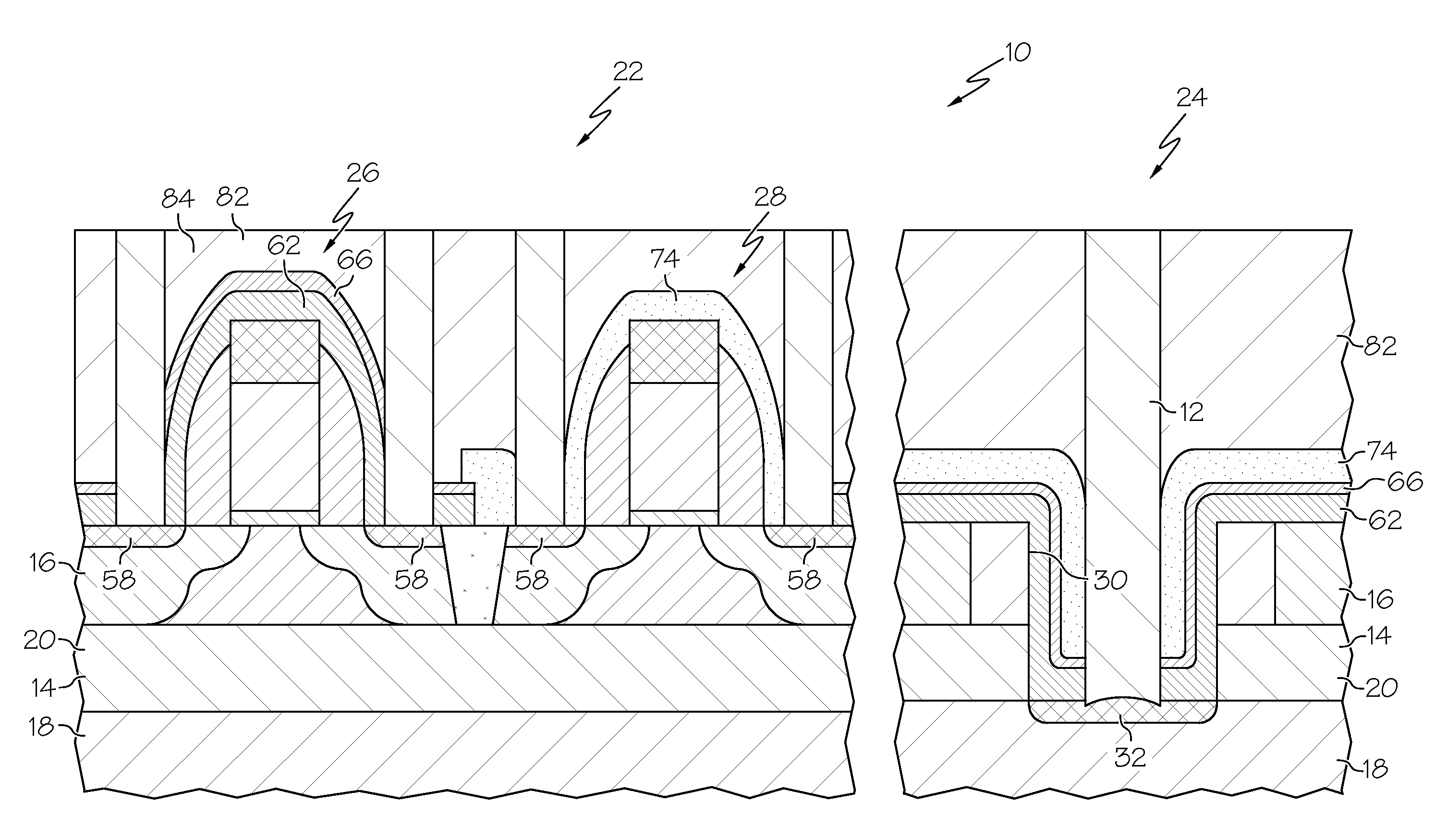
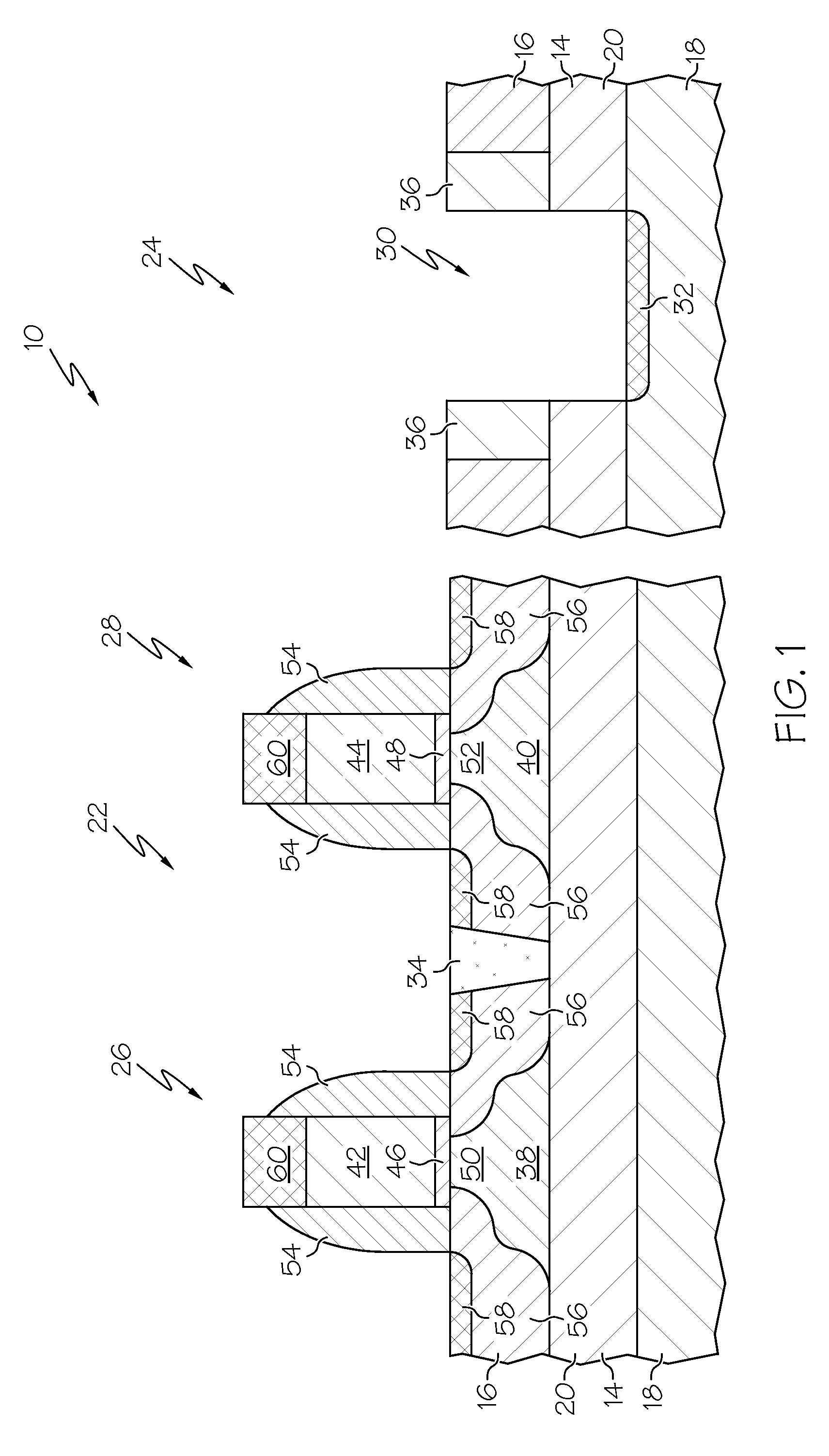
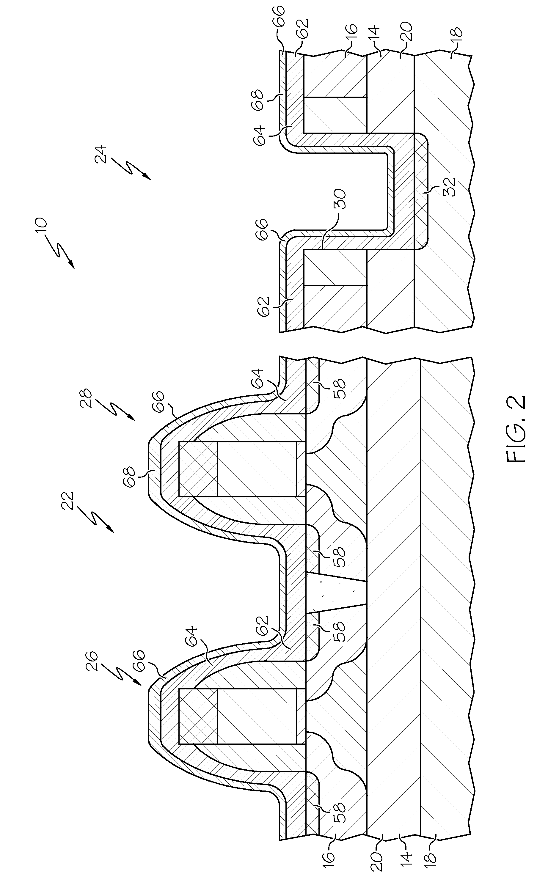
This patent describes methods for fabricating integrated circuits using a SOI substrate. The methods involve forming trenches in the substrate and filling them with a metal silicide region. A layer of stress-inducing material is placed over the metal silicide region, and an ILD layer of dielectric material is placed over the stress-inducing layers. A second trench is then formed to expose the metal silicide region and filled with a conductive material. The methods enable improved performance and reliability of the integrated circuits. Additionally, the patent provides an integrated circuit with a substrate contact that includes a metal silicide region and stress-inducing layers. Overall, the patent provides technical solutions for improving the fabrication of integrated circuits on SOI substrates.

Problems solved by technology

This configuration provides significant advantages but also give rise to certain issues.
One issue, especially in high performance devices such as microprocessors and the like, is that a thorough temperature sensing regime may be required across the substrate for device-internal temperature management because the buried insulating layer reduces the heat dissipation capabilities of the SOI devices.
This deeper interlayer dielectric material etch can be more challenging and sometimes results in the formation of substrate contacts that marginally extend to the silicon substrate, which can negatively impact the performance and robustness of the substrate contacts.

Method used


Image

  • Methods for fabricating integrated circuits having substrate contacts and integrated circuits having substrate contacts
  • Methods for fabricating integrated circuits having substrate contacts and integrated circuits having substrate contacts
  • Methods for fabricating integrated circuits having substrate contacts and integrated circuits having substrate contacts

Examples


Embodiment Construction

[0012]The following Detailed Description is merely exemplary in nature and is not intended to limit the invention or the application and uses of the invention. Furthermore, there is no intention to be bound by any theory presented in the preceding background or the following detailed description.

[0013]Various embodiments contemplated herein relate to methods for fabricating integrated circuits having substrate contacts and integrated circuits having substrate contacts. During intermediate stages of the fabrication of an integrated circuit (IC), a first stress-inducing layer is deposited over a first device region and a second device region of an SOI substrate. The SOI substrate has a semiconductor layer, a silicon substrate, and a buried insulating layer that is disposed between the semiconductor layer and the silicon substrate. The first device region has a first transistor and a second transistor that are formed in the semiconductor layer of the SOI substrate. The second device re...


PUM


Abstract

Methods for fabricating integrated circuits having substrate contacts and integrated circuits having substrate contacts are provided. One method includes forming a first trench in a SOI substrate extending through a buried insulating layer to a silicon substrate. A metal silicide region is formed in the silicon substrate exposed by the first trench. A first stress-inducing layer is formed overlying the metal silicide region. A second stress-inducing layer is formed overlying the first stress-inducing layer. An ILD layer of dielectric material is formed overlying the second stress-inducing layer. A second trench is formed extending through the ILD layer and the first and second stress-inducing layers to the metal silicide region. The second trench is filled with a conductive material.

Description

TECHNICAL FIELD[0001]The present invention relates generally to integrated circuits, and more particularly relates to methods for fabricating integrated circuits having substrate contacts and integrated circuits having substrate contacts.BACKGROUND[0002]Transistors such as metal oxide semiconductor field effect transistors (MOSFETs) or simply field effect transistors (FETs) or MOS transistors are the core building blocks of the vast majority of semiconductor integrated circuits (ICs). A FET includes source and drain regions between which a current can flow through a channel under the influence of a bias applied to a gate electrode that overlies the channel. The ICs are usually formed using both P-channel FETs (PMOS transistors or PFETs) and N-channel FETs (NMOS transistors or NFETs) and the IC is then referred to as a complementary MOS or CMOS circuit.[0003]Certain improvements in the performance of MOS ICs can be realized by forming the MOS transistors in a thin layer of semiconduc...

Claims


Application Information

Patent Timeline
IPC IPC(8): H01L21/768H01L23/48B82Y40/00
CPCH01L23/48H01L21/28518H01L21/743H01L21/76802H01L2924/0002H01L21/76816H01L2924/00
Inventor SCHEIPER, THILOFLACHOWSKY, STEFANHOENTSCHEL, JAN
Owner GLOBALFOUNDRIES US INC
Learn More