Integrated circuit chip with reduced ir drop

a technology of integrated circuit chip and ir drop, which is applied in the direction of semiconductor devices, semiconductor/solid-state device details, electrical apparatus, etc., can solve the problems of reducing signal timing speed and increasing power consumption, and achieve the effect of reducing metal layer resistance and lowering ir drop over an integrated circuit chip

Active Publication Date: 2013-10-10
MEDIATEK INC
View PDF1 Cites 1 Cited by
  • Summary
  • Abstract
  • Description
  • Claims
  • Application Information

AI Technical Summary

Benefits of technology

This patent aims to provide an interconnection structure that can be used in semiconductor manufacturing processes and reduce metal layer resistance, which can lower the thermal response of the integrated circuit chip and improve its performance. The text also mentions the use of metal-insulator-metal or MIM-like structures to achieve the same goal.

Problems solved by technology

However, this approach unavoidably induces high voltage drop (or IR drop), which results in increased power consumption and reduced signal timing speed.

Method used


Image

  • Integrated circuit chip with reduced ir drop
  • Integrated circuit chip with reduced ir drop
  • Integrated circuit chip with reduced ir drop

Examples


Embodiment Construction

[0021]Certain terms are used throughout the description and following claims to refer to particular components. As one skilled in the art will appreciate, electronic equipment manufacturers may refer to a component by different names. This document does not intend to distinguish between components that differ in name but not function. In the following description and in the claims, the terms “include” and “comprise” are used in an open-ended fashion, and thus should be interpreted to mean “include, but not limited to . . . ”. Also, the term “couple” is intended to mean either an indirect or direct electrical connection. Accordingly, if one device is coupled to another device, that connection may be through a direct electrical connection, or through an indirect electrical connection via other devices and connections.

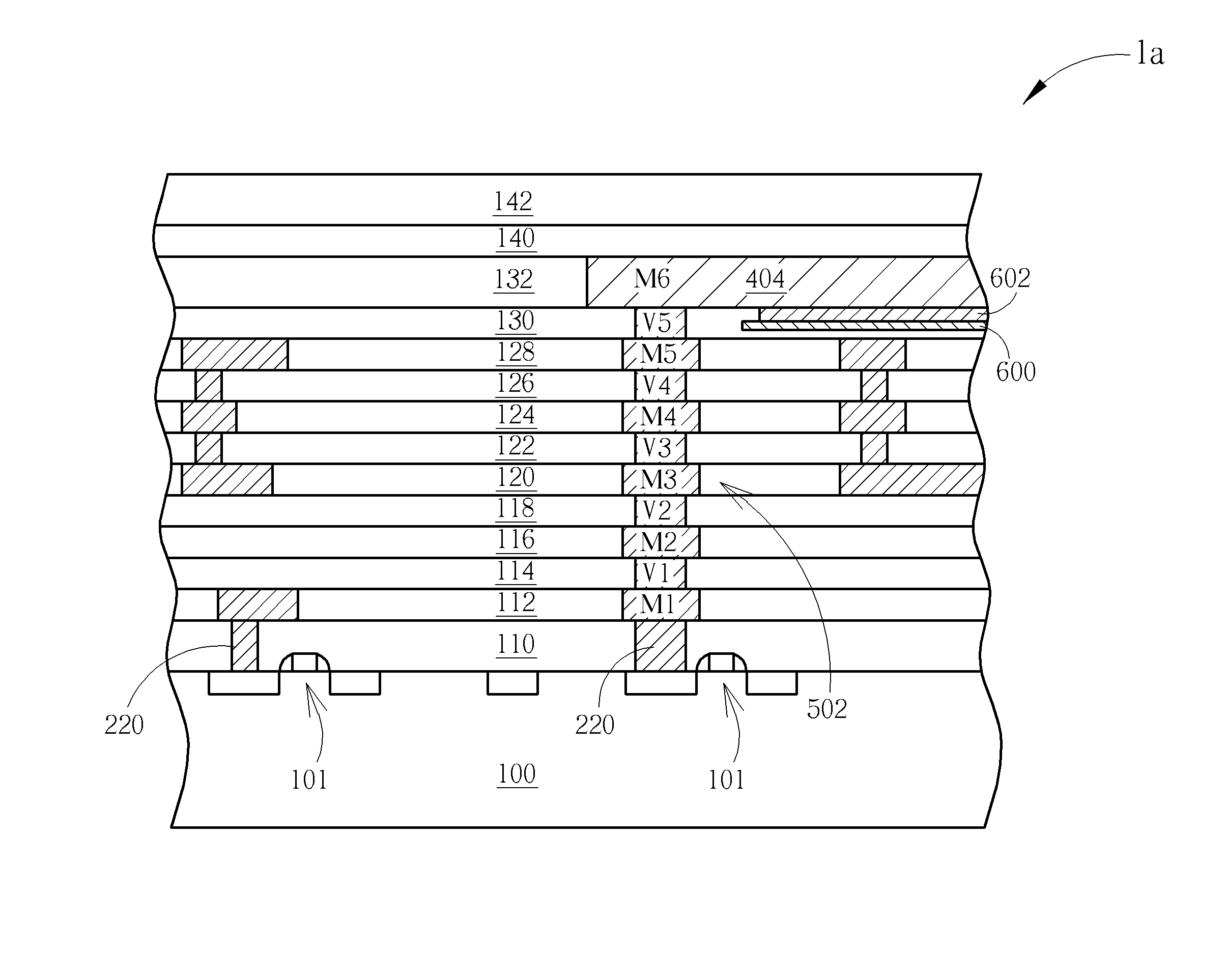
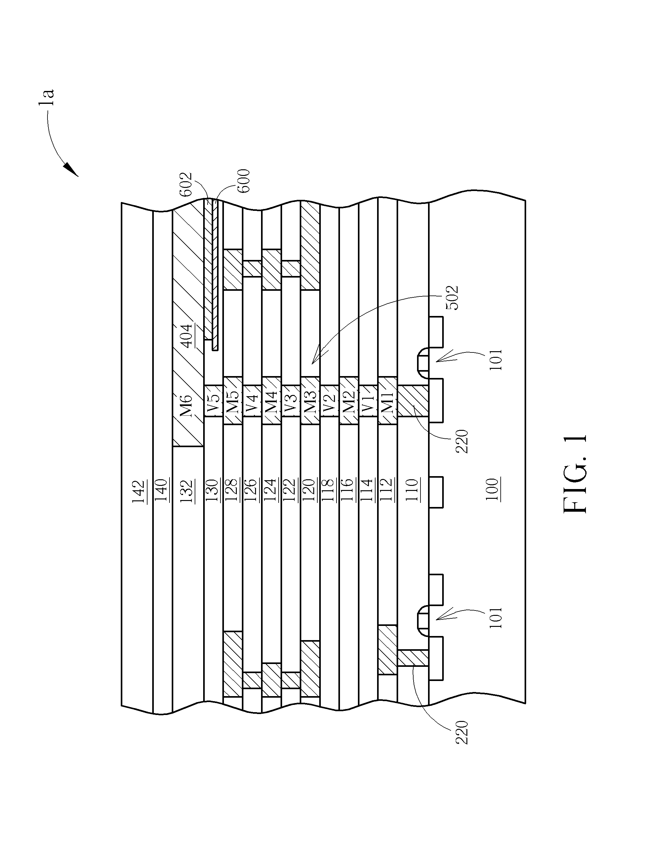
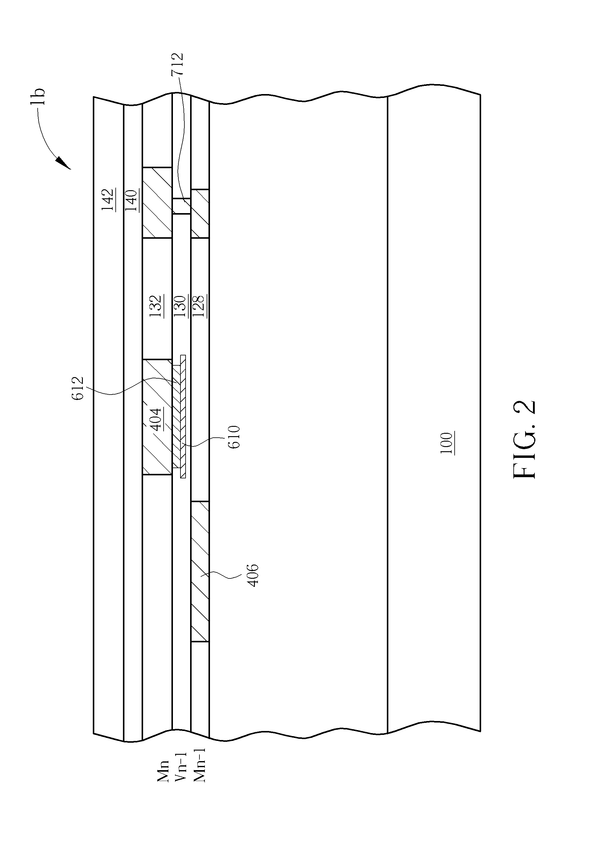
[0022]The present invention pertains to an interconnection structure that is compatible with current semiconductor manufacturing process and is capable of reducing the me...


PUM


Abstract

An integrated circuit chip includes a semiconductor substrate; a first interconnection wire having a first portion and a second portion on the semiconductor substrate, wherein the second portion is separated from the first portion; a second interconnection wire situated under the first interconnection wire; a first conductive via electrically coupling the first portion with the second interconnection wire; a conductive layer situated between the first interconnection wire and the second interconnection wire; and a second conductive via electrically coupling the conductive layer with the second portion.

Description

CROSS REFERENCE TO RELATED APPLICATIONS[0001]This is a continuation-in-part of U.S. application Ser. No. 12 / 435,398 filed May 4, 2009, which is incorporated herein by reference for all purposes.BACKGROUND OF THE INVENTION[0002]1. Field of the Invention[0003]The present invention relates generally to the field of semiconductor integrated circuit devices. More particularly, the present invention relates to an improved integrated circuit chip and its interconnection scheme that are capable of reducing IR drop over the chip.[0004]2. Description of the Prior Art[0005]In the processes for designing a large-scale integrated semiconductor circuit device, respective blocks of the device are generally designed in parallel to complement device characteristics with one another. During the designing the large-scale device, the building-block type of method is utilized, in which the circuit of the device is divided into a plurality of circuit blocks and each of the circuit blocks is thus designed...

Claims


Application Information

Patent Timeline
Patent Type & Authority Applications(United States)
IPC IPC(8): H01L23/538H10N97/00
CPCH01L23/5223H01L23/5286H01L23/5384H01L21/00H01L23/00H01L2924/0002H01L27/00H01L28/00H01L2924/00
Inventor TU, CHAO-CHUNLIN, SHIH-HUNGHUANG, CHIH-CHIENCHANG, TIEN-CHANG
Owner MEDIATEK INC
Why Eureka
Try Eureka