Lens array and optical module including the same

a technology of optical modules and arrays, applied in the field of lenses arrays and optical modules, can solve problems such as the risk of disruption in the appropriate transmission of communication information, and achieve the effect of improving the temperature stability and the optical performance of the sam

Active Publication Date: 2013-10-10
ENPLAS CORP
View PDF10 Cites 39 Cited by
  • Summary
  • Abstract
  • Description
  • Claims
  • Application Information

AI Technical Summary

Benefits of technology

[0057]In the present invention, appropriate attachment of the photovoltaic device taking into consideration deformation of the lens array main body caused

Problems solved by technology

In addition, since the past, the photovoltaic device attached to this type of lens array has been problematic in that, as a result of changes in the output characteristics of th

Method used


Image

  • Lens array and optical module including the same
  • Lens array and optical module including the same
  • Lens array and optical module including the same

Examples


first embodiment

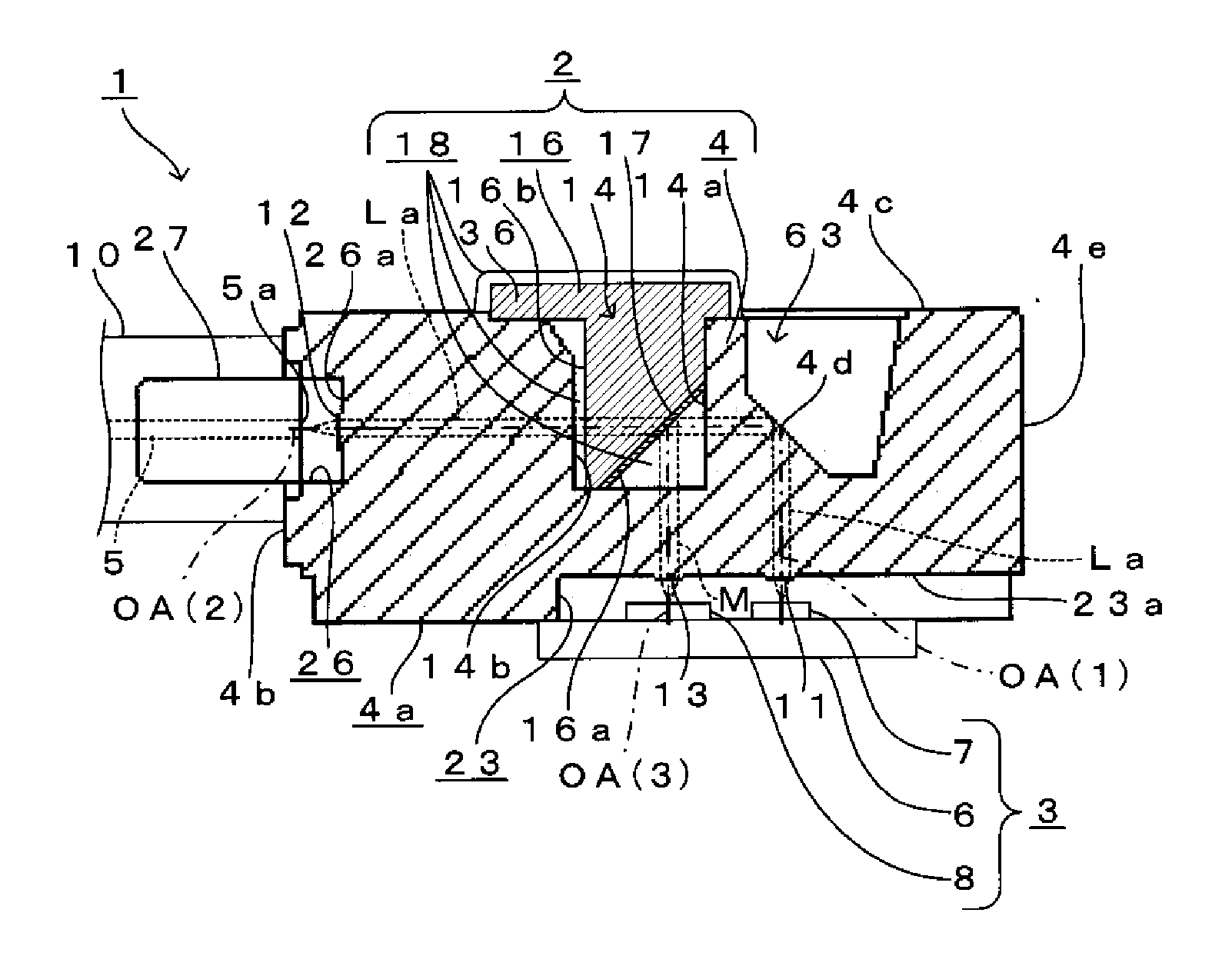
[0164]A lens array and an optical module including the lens array according to a first embodiment of the present invention will hereinafter be described with reference to FIG. 1 to FIG. 18.

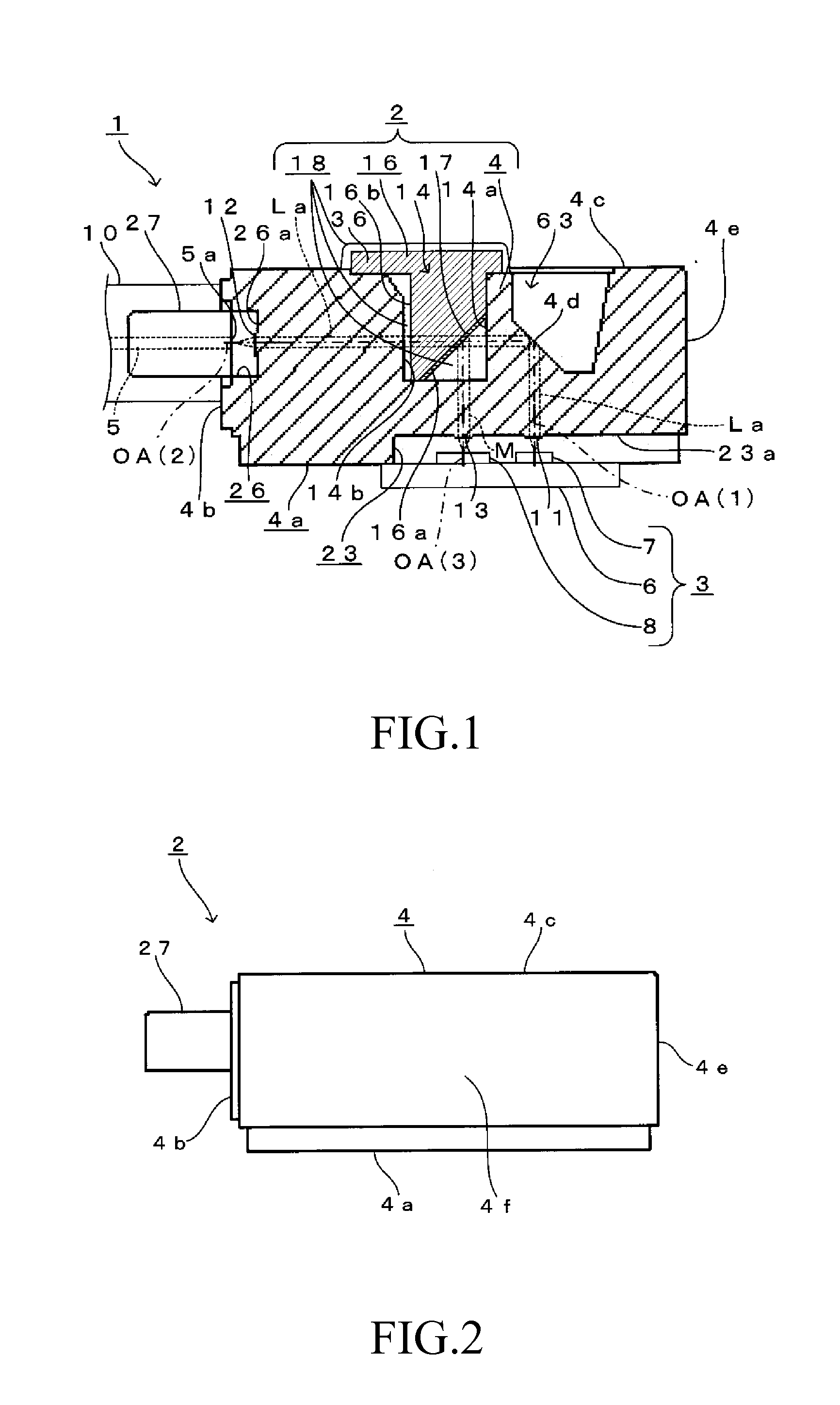
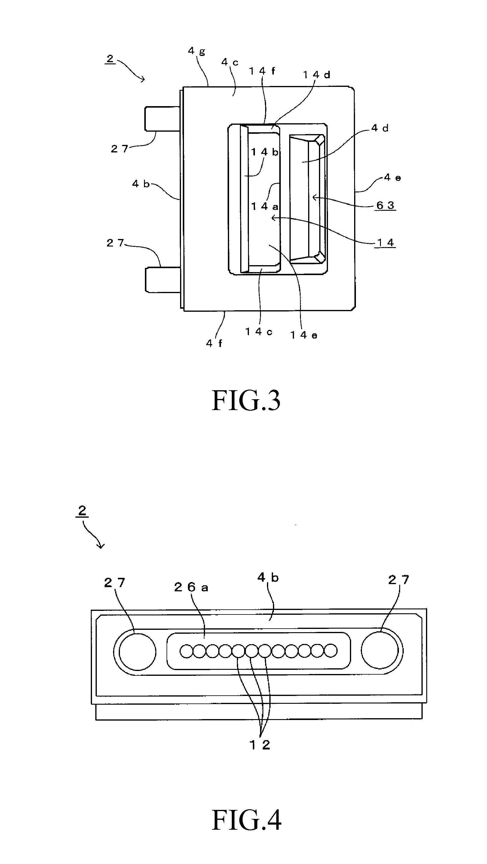
[0165]Here, FIG. 1 is an overall configuration diagram of an overview of an optical module 1 according to the present embodiment, together with a vertical cross-sectional view of a lens array 2 according to the present embodiment. In addition, FIG. 2 is a front view of the lens array 2 shown in FIG. 1. FIG. 3 is a planar view of the lens array 2 shown in FIG. 1. FIG. 4 is a left-side view of the lens array 2 shown in FIG. 1. FIG. 5 is a right-side view of the lens array 2 shown in FIG. 1. FIG. 6 is a bottom view of the lens array 2 shown in FIG. 1.

[0166]As shown in FIG. 1, the lens array 2 according to the present embodiment is disposed between a photovoltaic device 3 and optical fibers 5.

[0167]Here, the photovoltaic device 3 has a plurality of light-emitting elements 7 on a surface of a semicondu...

examples

[0232]Examples of the present invention will be described with reference to FIG. 10 and FIG. 11.

[0233]FIG. 10 shows the simulation results for optical coupling efficiency using the lens array 2 based on design between light-emitting sections (light-emitting elements) of a VCSEL including a monitor PD as the photovoltaic device 3 and the end faces 5a of multi-mode optical fibers 5 having a diameter of 50 μm, as specific simulation results for determining the first tolerance W1.

[0234]The vertical axis in FIG. 10 indicates the optical coupling efficiency between the VCSEL and the fibers as coupling loss (dB). The horizontal axis in FIG. 10 indicates a movement width [μm] from a point of origin under a premise that the VCSEL is moved in the direction perpendicular to the optical axis OA(1) of the first lens faces 11 from the attachment position (point of origin on the horizontal axis) to the lens array 2 at which the optical coupling efficiency becomes the maximum efficiency based on de...

second embodiment

[0264]Next, a lens array and an optical module including the lens array according to a second embodiment of the present invention will be described with reference to FIG. 19 to FIG. 87, mainly focusing on the differences with the first embodiment.

[0265]Sections of which the basic configuration is the same or similar to that according to the first embodiment are described using the same reference numbers.

[0266]FIG. 19 is a front view of the lens array 2 according to the present embodiment. FIG. 20 is a planar view of FIG. 19. FIG. 21 is a bottom view of FIG. 19. The left-side view of FIG. 19 is similar to FIG. 4.

[0267]The lens array 2 according to the present embodiment is used to optically couple the photovoltaic device 3 and the optical fibers 5 in a state in which the photovoltaic device 3 and the optical fibers 5 are attached to the lens array 2 (not shown), in a manner similar to that according to the first embodiment.

[0268]However, as shown in FIG. 19 to FIG. 21, unlike that ac...


PUM


Abstract

A lens array satisfies a+b+d1+e+ΔL≦W1 where:
    • a: positional accuracy of first lens faces 11,
    • b: positional accuracy of second lens faces 12,
    • d1: positional accuracy of light-emitting elements 7,
    • e: positional accuracy of optical fibers 5,
    • ΔL=α×ΔT×L (α: coefficient of linear expansion of lens array main body 4; ΔT: temperature change in the lens array main body 4; and L: distance from a fixed position on a first surface 4a to a position of a lens face on the first surface 4a farthest from the fixed position),
    • W1: a distance between attachment positions before and after movement, under a premise that a photovoltaic device 3 is moved from an attachment position at which optical coupling efficiency between the light-emitting elements 7 and fiber ends 5a indicates a maximum efficiency to an attachment position at which efficiency reduction equivalent to 2 dB is indicated.

Description

TECHNICAL FIELD[0001]The present invention relates to a lens array and an optical module including the lens array. In particular, the present invention relates to a lens array suitable for optically coupling a plurality of light-emitting elements and end faces of a plurality of optical fibers, and an optical module including the lens array.BACKGROUND ART[0002]In recent years, in reflection of the need for higher-speed communication and more compact communication devices, there has been an increasing demand for a lens array in which a plurality of lenses are arranged in parallel, as a compactly structured optical component effective for actualizing multichannel optical communication.[0003]This type of lens array is conventionally configured such that a photovoltaic device including a plurality of light-emitting elements (such as a vertical cavity surface emitting laser [VCSEL]) can be attached thereto and a plurality of optical fibers can be attached thereto.[0004]In a state in which...

Claims


Application Information

Patent Timeline
IPC IPC(8): G02B6/42
CPCG02B6/325G02B6/4214G02B6/4249G02B6/4246G02B6/4292G02B6/42G02B6/4286
Inventor MORIOKA, SHIMPEINIIMI, TADANOBUSHIBUYA, KAZUTAKA
Owner ENPLAS CORP
Why Eureka
Try Eureka