

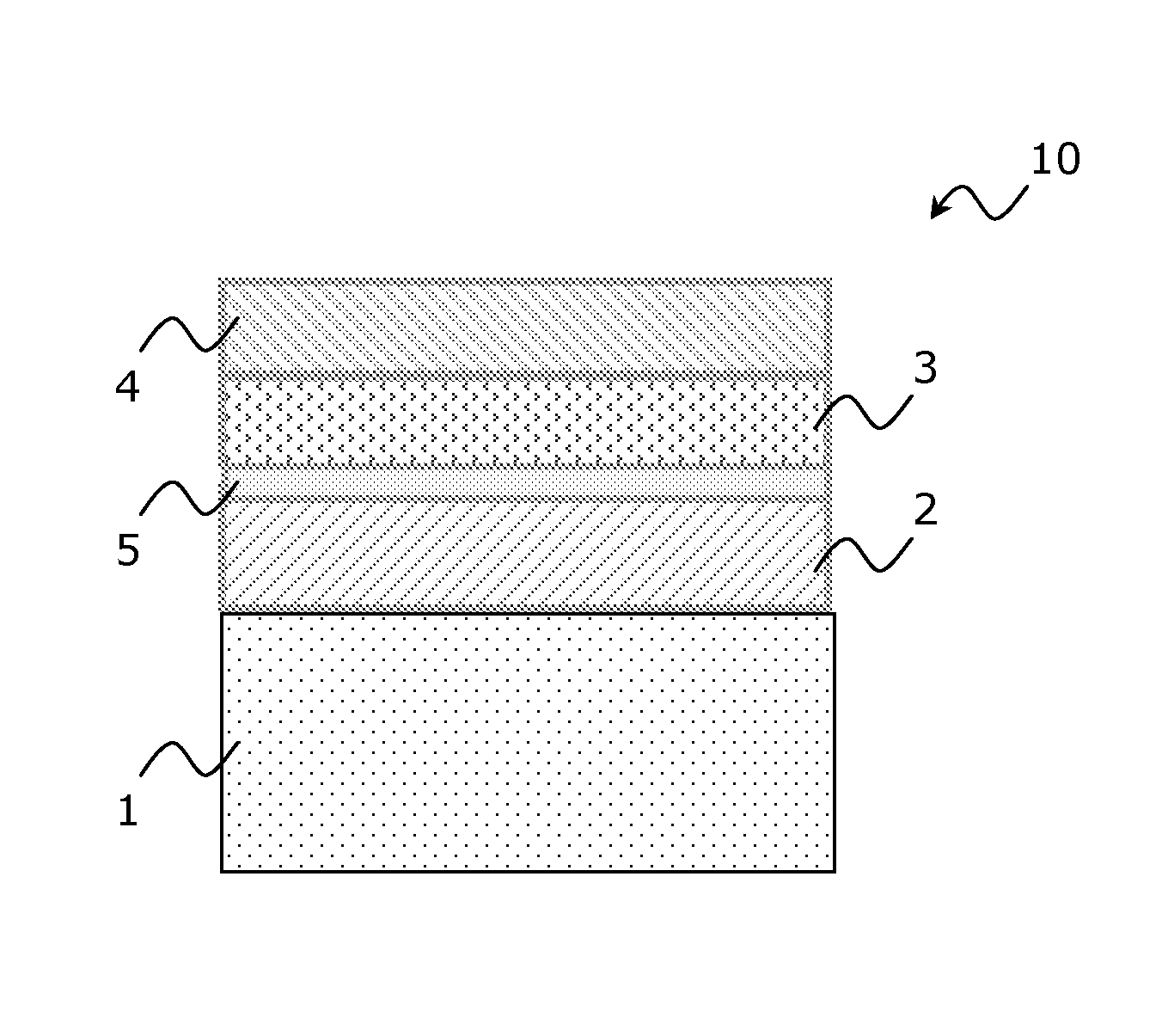
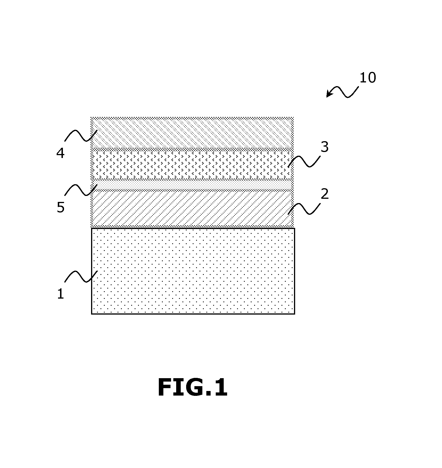
Microelectronic device with programmable memory, including a layer of doped chalcogenide that withstands high temperatures
a microelectronic device and programmable memory technology, applied in the direction of bulk negative resistance effect devices, basic electric elements, electric devices, etc., can solve the problems of loss of electrical performance, short circuits, and significant drop in glass transition temperatur
- Summary
- Abstract
- Description
- Claims
- Application Information
AI Technical Summary
Benefits of technology
Problems solved by technology
Method used
Image

Examples
examples
[0115]A series of tests were performed by simulating the heat budget encountered during industrial fabrication of a CBRAM stack by vacuum annealing for 15 minutes at temperatures lying in the range 300° C. to 450° C.
[0116]The CBRAM stacks made were of the type shown in FIG. 1, with a few differences, namely:
[0117]a stack E1 identical to that of FIG. 1, except that it did not have an intermediate layer of ruthenium;
[0118]a stack E2 identical to that of FIG. 1, except that the intermediate layer of ruthenium (Ru) was replaced by a layer of tantalum (Ta);
[0119]a stack E3 identical to that of FIG. 1, except that the intermediate layer of ruthenium (Ru) was replaced by a layer of tantalum nitride (TaN);
[0120]a stack E4 identical to that of FIG. 1, except that the intermediate layer of ruthenium (Ru) was replaced by a layer of platinum (Pt); and
[0121]a stack E5 identical to that of FIG. 1, in accordance with the invention.
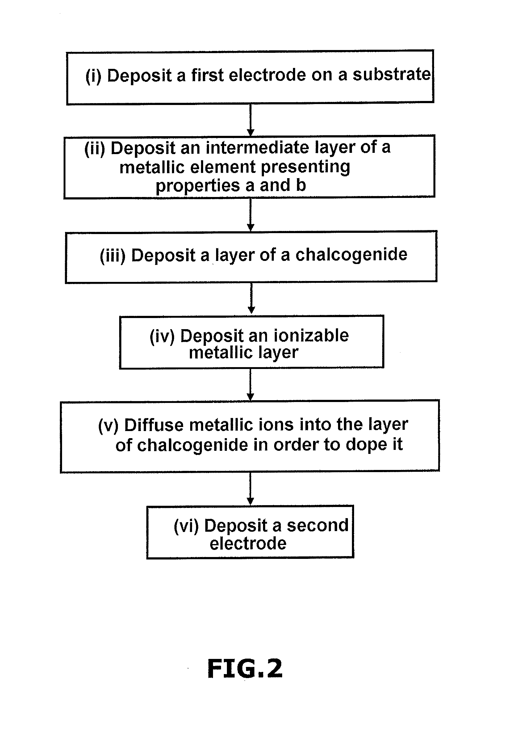
[0122]The operating conditions for depositing the layers constituti...
PUM
| Property | Measurement | Unit |
|---|---|---|
| coefficient of thermal conductivity | aaaaa | aaaaa |
| thickness | aaaaa | aaaaa |
| temperatures | aaaaa | aaaaa |
Abstract
Description
Claims
Application Information