In-cell multi-touch display panel system

Active Publication Date: 2013-10-31
FOCALTECH SYSTEMS LTD
View PDF22 Cites 44 Cited by
  • Summary
  • Abstract
  • Description
  • Claims
  • Application Information

AI Technical Summary

Benefits of technology

[0031]The object of the present invention is to provide an in-cell multi-touch display panel system, which can overcome the prior problem of limiting the increased resolutio

Problems solved by technology

The surface capacitive touch sensing has a simple configuration, but the multi-touch implementation is not easy, and the problems of electromagnetic disturbance (EMI) and noises are difficult to be overcome.
(3) lower power consumption due to the reduced amount of data to be processed.
However, such a self capacitance sensing also has the disadvantages as follows:
(1) When there is a floating conductor (such as a water drop, an oil stain, and the like) on the touch panel, it may causes an error decision on a touch point; and
(2) When there are multiple touch points concurrently on the touch panel, it may cause a ghost point effect, resulting in that such a self capacitance sensing cannot be used in multi-touch applications.
However, such a way requires an increase of the weight o

Method used


Image

  • In-cell multi-touch display panel system
  • In-cell multi-touch display panel system
  • In-cell multi-touch display panel system

Examples


Embodiment Construction

[0044]FIG. 5 is a block diagram of an in-cell multi-touch display panel system 500 according to the invention. The in-cell multi-touch display panel 500 includes a touch LCD panel 510 and a touch display control subsystem 520.

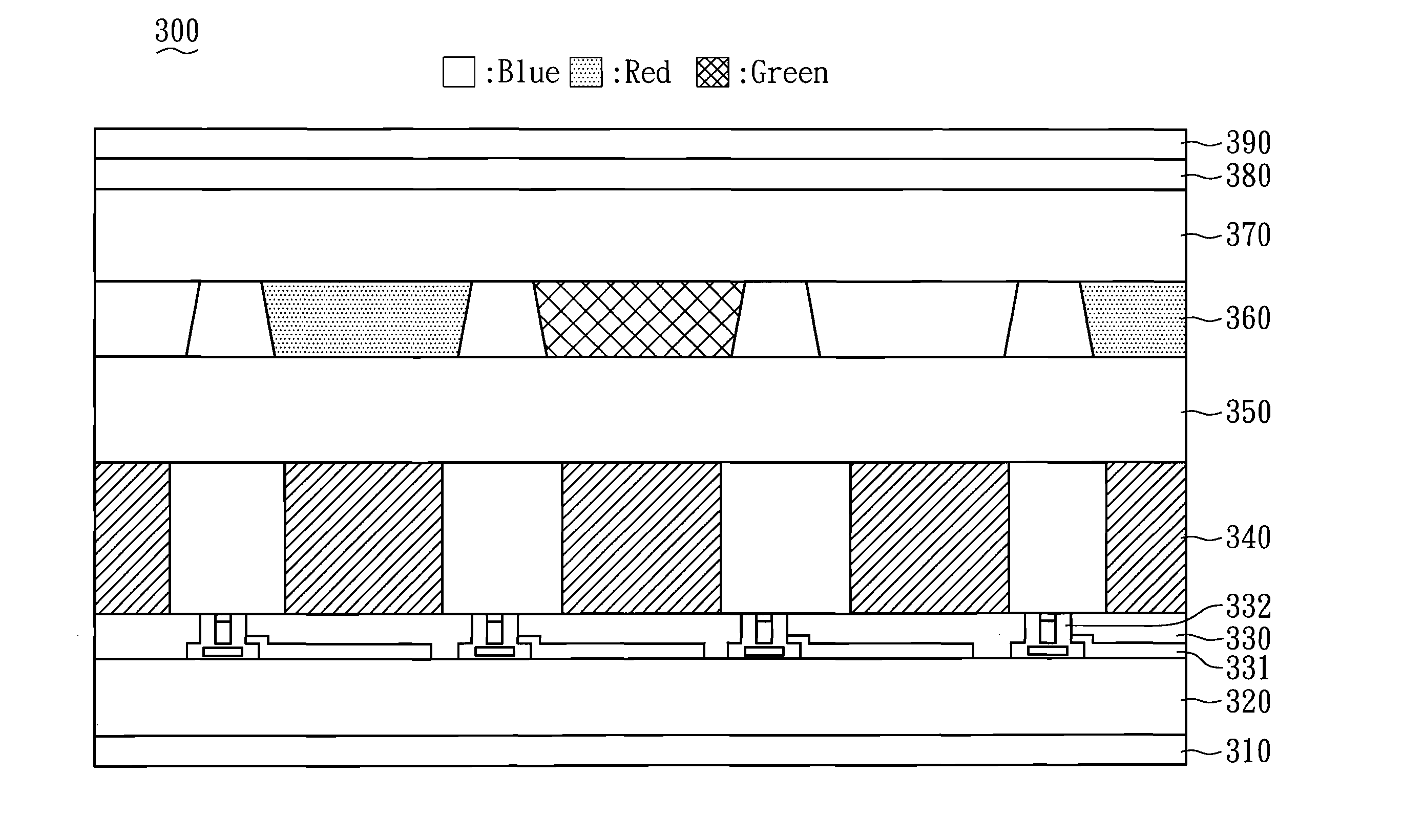
[0045]The touch LCD panel 510 has a thin film transistor (TFT) layer 330, a conductive electrode layer 380, and a common-voltage and touch-driving layer 350, wherein the three layers 330, 350 and 380 can be combined and stacked into one of the configurations shown in FIGS. 3(A)-3(D).

[0046]The TFT layer 330 has K gate driving lines (G1, G2, . . . , GK) and L source driving lines (SOURCE1, SOURCE2, . . . , SOURCEL) in order to drive transistors and capacitors corresponding to pixels of the LCD panel 510 based on a display pixel signal and a display driving signal in display, where K, L are each a positive integer. For convenience of description, in this embodiment, we have K=800 and L=600.

[0047]The active element of the TFT transistor layer 330 is the TFT in this...


PUM


Abstract

An in-cell multi-touch display panel system includes a touch LCD panel and a touch display control subsystem. The touch LCD panel has a TFT layer, a conductive electrode layer, and a common-voltage and touch-driving layer. The TFT layer has K gate driving lines and L source driving lines for a display operation. The conductive electrode layer has M first conduct lines for a touch detection operation by sampling a touch detection result from the M first conduct lines. The common-voltage and touch-driving layer has N second conduct lines for receiving a common voltage signal in display and receiving a touch-driving signal in touch detection. The K gate driving lines are divided into N groups respectively corresponding to the N second conduct line. When one group of gate driving lines has the display driving signal, the corresponding second conduct line is connected to the common voltage signal.

Description

BACKGROUND OF THE INVENTION[0001]1. Field of the Invention[0002]The present invention relates to the technical field of touch panels and, more particularly, to an in-cell multi-touch display panel system.[0003]2. Description of Related Art[0004]The principle of touch panels is based on different sensing manners to detect a voltage, current, acoustic wave, or infrared to thereby detect the coordinate of a touch point on a screen as touched by a finger or other objects. For example, a resistive touch panel uses a voltage difference between the upper and lower electrodes to compute the position of a pressed point for detecting the location of the touch point, and a capacitive touch panel uses a capacitance change generated in an electrostatic combination of the arranged transparent electrodes with the touching part of a human body to generate a current or voltage for detecting the coordinate of the touching part.[0005]Upon the principle, the capacitive touch technologies can be divided...

Claims


Application Information

Patent Timeline
IPC IPC(8): G09G3/36
CPCG09G3/3611G06F3/0412G06F3/04166G06F3/0443G06F2203/04103G06F3/047G06F2203/04104
Inventor HUANG, CHIEN-YINGHUANG, YEN-LIN
Owner FOCALTECH SYSTEMS LTD
Why Eureka
Try Eureka