Optical components having a common etch depth

a technology of optical components and depths, applied in the direction of optical light guides, optical waveguide light guides, instruments, etc., can solve the problems of waveguides also significantly increasing the optical scattering loss at the optical-waveguide core-cladding boundary, and the approach contradicts the requirements of high-density routing and low-power active devices

Active Publication Date: 2013-11-14
ORACLE INT CORP
View PDF14 Cites 13 Cited by
  • Summary
  • Abstract
  • Description
  • Claims
  • Application Information

AI Technical Summary

Problems solved by technology

Although optical-waveguide crossings can potentially be made with very low optical loss (for example, approximately 0.1 dB) and low crosstalk (such as −40 dB), they typically present severe constraints to the scaling of an optical communication network because a large number of optical-waveguide crossings may be needed for routing in a single photonic layer.
While silicon optical waveguides can enable very compact optical devices, and thus can help provide low-power and high-density optical links, these optical waveguides also usually significantly increase the optical scattering loss at the optical-waveguide core-cladding boundary.
However, this approach contradicts the requirements of high-density routing and low-power active devices.

Method used


Image

  • Optical components having a common etch depth
  • Optical components having a common etch depth
  • Optical components having a common etch depth

Examples


Embodiment Construction

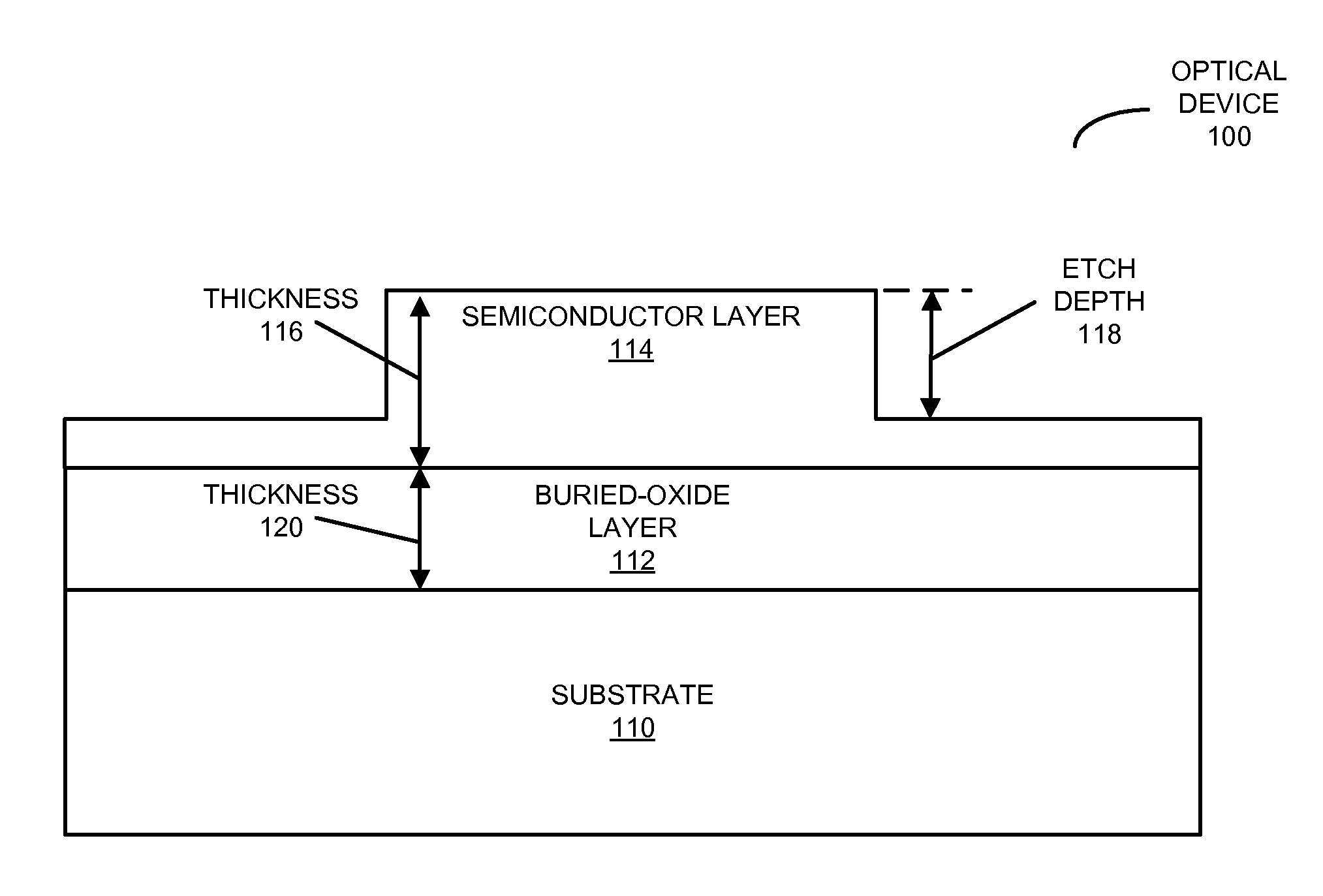
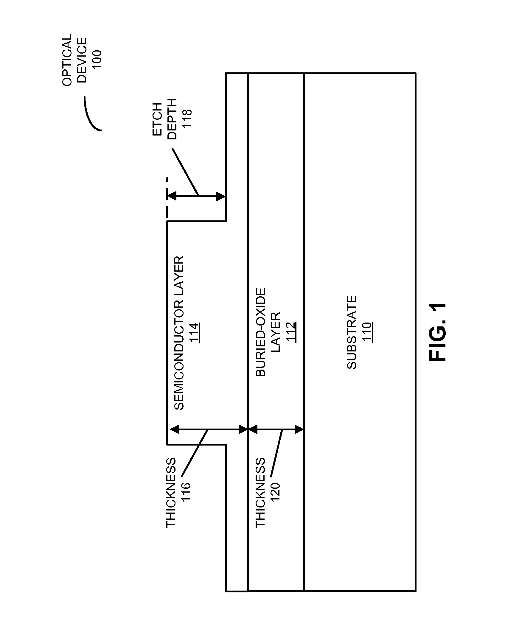
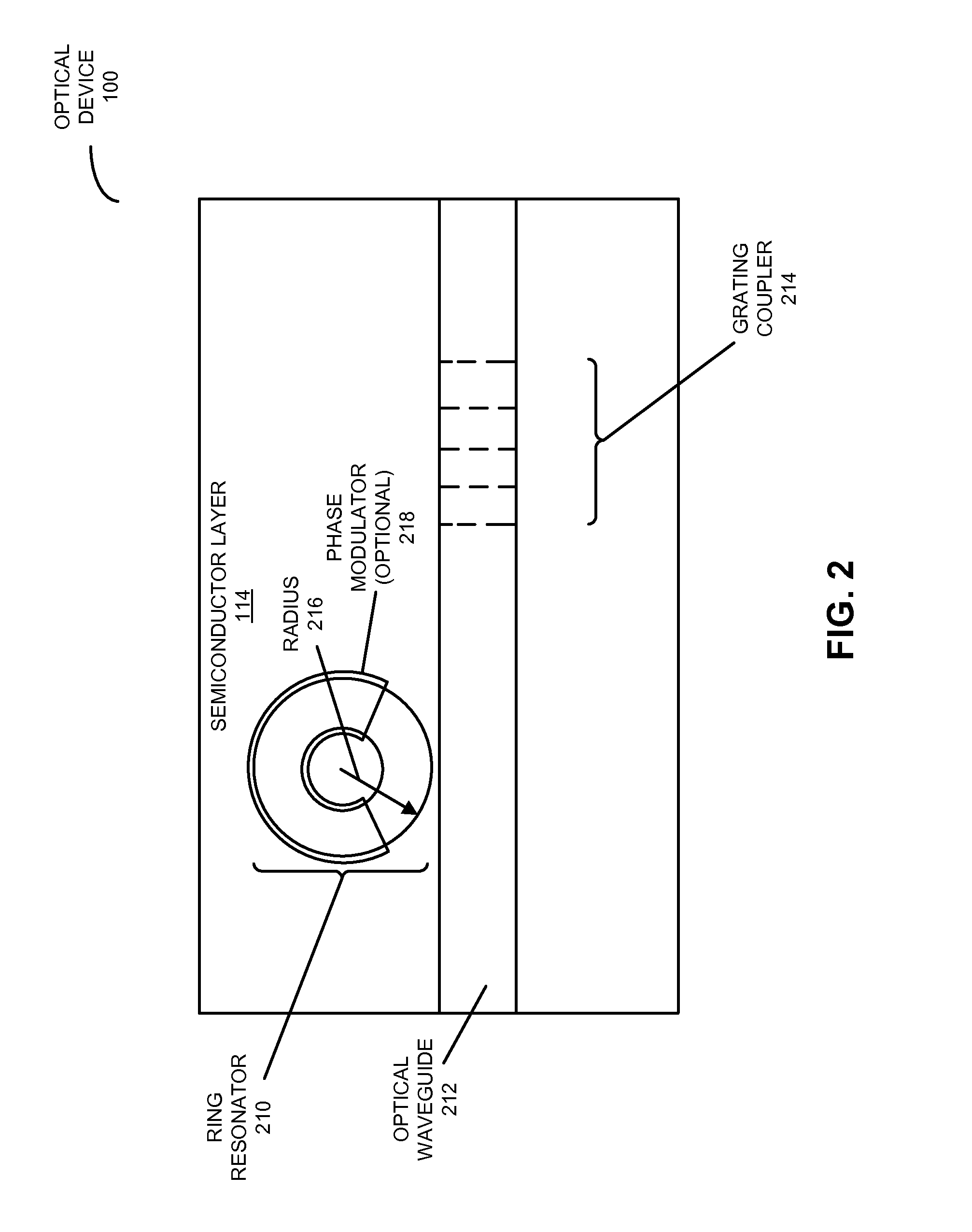
[0024]Embodiments of an optical device, a system that includes the optical device, and a technique for fabricating the optical device are described. The optical device includes multiple components, such as a ring resonator, an optical waveguide and a grating coupler, having a common etch depth (which is associated with a single etch step or operation during fabrication). Moreover, these components may be implemented in a semiconductor layer in a silicon-on-insulator technology.

[0025]By using a common etch depth, this fabrication technique may simultaneously produce: compact active devices, multimode optical waveguides (including optical waveguides with tight bends, ultralow-loss routing optical waveguides, and optical-waveguide taper regions), high-speed ring resonator modulators with ultralow power consumption, and compact low-loss interlayer couplers for multilayer-routed optical links. The wide routing optical waveguide can be tightly spaced, for example, with a 5 μm pitch. This ...


PUM


Abstract

An optical device is described. This optical device includes multiple components, such as a ring resonator, an optical waveguide and a grating coupler, having a common etch depth (which is associated with a single etch step or operation during fabrication). Moreover, these components may be implemented in a semiconductor layer in a silicon-on-insulator technology. By using a common etch depth, the optical device may provide: compact active devices, multimode ultralow-loss optical waveguides, high-speed ring resonator modulators with ultralow power consumption, and compact low-loss interlayer couplers for multilayer-routed optical links. Furthermore, the single etch step may help reduce or eliminate optical transition loss, and thus may facilitate high yield and low manufacturing costs.

Description

CROSS REFERENCE TO RELATED APPLICATION[0001]This application claims priority under 35 U.S.C. §119(e) to U.S. Provisional Application Ser. No. 61 / 646,094, entitled “Enabling Multi-Layer-Routed Si-Photonic Links Using Single Step Waveguide Etching,” by Guoliang Li, Xuezhe Zheng, and Ashok V. Krishnamoorthy, Attorney Docket No. ORA12-0777PSP2, filed on May 11, 2012, the contents of which is herein incorporated by reference.GOVERNMENT LICENSE RIGHTS[0002]This invention was made with Government support under Agreement No. HR0011-08-9-0001 awarded by DARPA. The Government has certain rights in the invention.BACKGROUND[0003]1. Field[0004]The present disclosure relates to the design of an optical device. More specifically, the present disclosure relates to the design of an optical device that includes components having a common etch depth.[0005]2. Related Art[0006]Engineers are beginning to investigate possible designs for a multi-chip module (which is sometimes referred to as a ‘macrochip’...

Claims


Application Information

Patent Timeline
Patent Type & Authority Applications(United States)
IPC IPC(8): G02B6/136G02B6/122
CPCG02B6/136G02B6/122G02B6/12004G02B6/12007G02B6/125
Inventor LI, GUOLIANGZHENG, XUEZHEKRISHNAMOORTHY, ASHOK V.
Owner ORACLE INT CORP
Why Eureka
Try Eureka