Optical memory system including an optically connected memory module and computing system including the same

a technology of optical connection and memory module, which is applied in the direction of optical elements, multiplex communication, instruments, etc., can solve the problems of limited number of memory modules coupled to the memory controller, the signal integrity of the electrical signal may further deteriorate, and the signal integrity of the electrical signal may be further deteriorated, so as to achieve efficient increase the system memory capacity

Active Publication Date: 2013-11-21
SAMSUNG ELECTRONICS CO LTD
View PDF13 Cites 21 Cited by
  • Summary
  • Abstract
  • Description
  • Claims
  • Application Information

AI Technical Summary

Benefits of technology

[0007]Some example embodiments provide an optical memory system capable of efficiently increasing a system memory capacity.
[0008]Some example embodiments provide a computing system capable of efficiently increasing a system memory capacity.

Problems solved by technology

In a conventional computing system where an electrical signal is transferred between a memory controller and a memory module, signal integrity of the electrical signal may deteriorate due to an impedance mismatch.
The signal integrity of the electrical signal may further deteriorate as the transfer speed of the electrical signal increases.
The number of memory modules coupled to the memory controller may be limited due to such deterioration of the signal integrity.
However, in a computing system including such an optically connected memory module, as the number of optically connected memory modules increases, the number of required light sources may increase, which results in the increase of a cost and power consumption.
Accordingly, the number of optically connected memory modules coupled to the memory controller may be limited.

Method used


Image

  • Optical memory system including an optically connected memory module and computing system including the same
  • Optical memory system including an optically connected memory module and computing system including the same
  • Optical memory system including an optically connected memory module and computing system including the same

Examples


Embodiment Construction

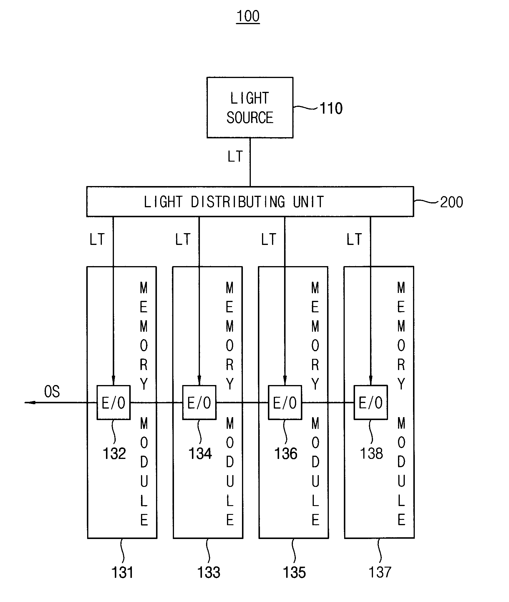
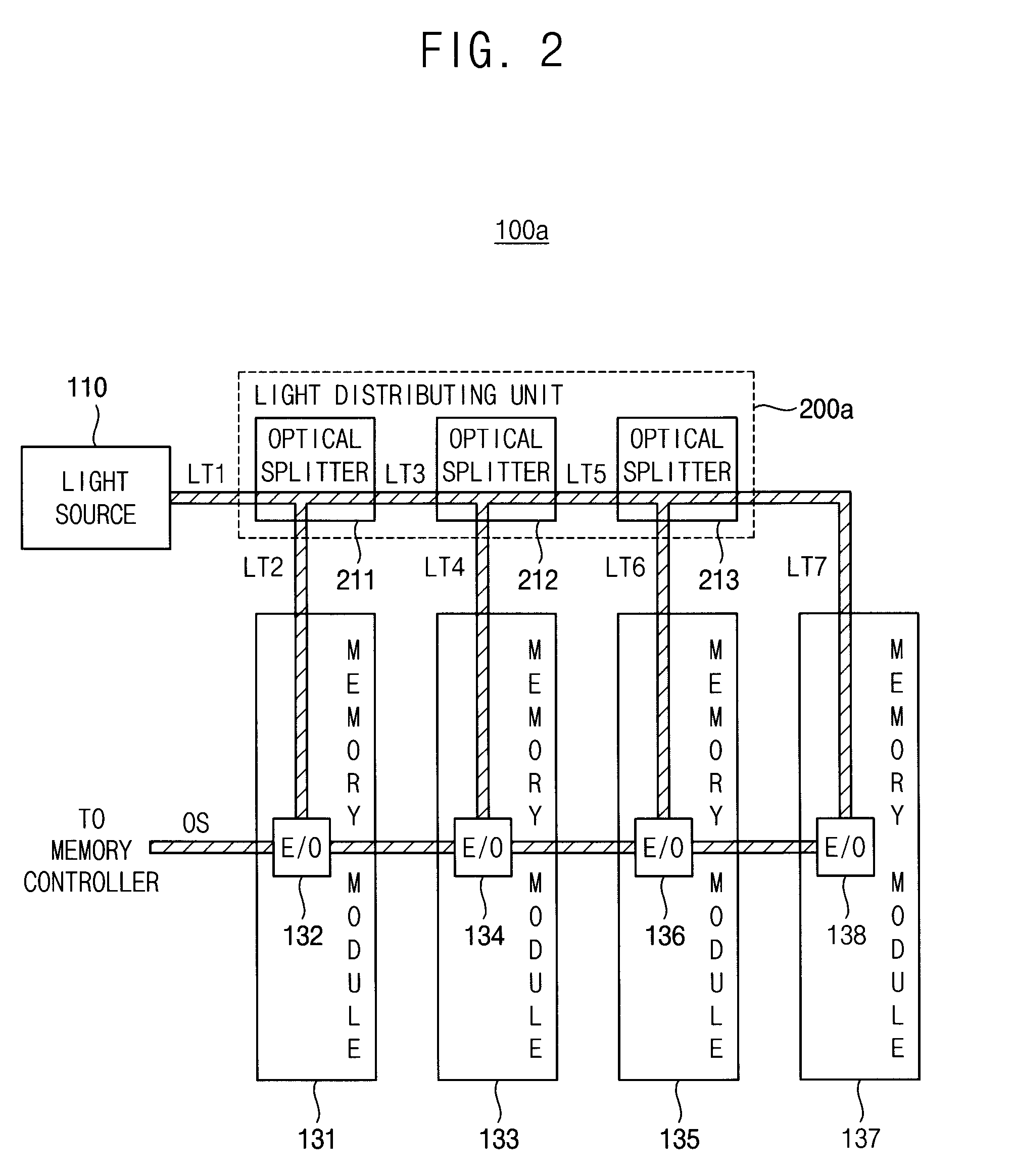
[0048]Various example embodiments will be described more fully hereinafter with reference to the accompanying drawings, in which some example embodiments are shown. The present inventive concept may, however, be embodied in many different forms and should not be construed as limited to the example embodiments set forth herein. In the drawings, the sizes and relative sizes of layers and regions may be exaggerated for clarity.

[0049]It will be understood that when an element or layer is referred to as being “on,”“between,”“connected to” or “coupled to” another element or layer, it can be directly on, connected or coupled to or between the other element or layer or intervening elements or layers may be present. In contrast, when an element is referred to as being “directly on,”“directly connected to” or “directly coupled to” another element or layer, there are no intervening elements or layers present.

[0050]Like numerals refer to like elements throughout. As used herein, the term “and / o...


PUM


Abstract

An optical memory system according to example embodiments includes a plurality of memory modules, each memory module including a plurality of memory devices; a light source; a light distribution unit connected to the light source through a first optical transmission line; a plurality of second optical transmission lines connected between the light distribution unit and the plurality of memory modules; a plurality of electrical to optical converters, each connected to at least one of the second optical transmission lines; and a plurality of output optical transmission lines connected to the plurality of electrical to optical converters, each output optical transmission line for outputting an electrical to optical converted signal.

Description

CROSS-REFERENCE TO RELATED APPLICATIONS[0001]This U.S. non-provisional application claims the benefit of priority under 35 U.S.C. §119 to Korean Patent Application No. 10-2012-0053556 filed on May 21, 2012 in the Korean Intellectual Property Office (KIPO), the entire content of which is incorporated by reference herein in its entirety.BACKGROUND[0002]1. Technical Field[0003]Example embodiments relate to optically connected memory modules. More particularly, example embodiments relate to optical memory systems including the optically connected memory modules and computing systems including the optical memory systems.[0004]2. Description of the Related Art[0005]In a conventional computing system where an electrical signal is transferred between a memory controller and a memory module, signal integrity of the electrical signal may deteriorate due to an impedance mismatch. The signal integrity of the electrical signal may further deteriorate as the transfer speed of the electrical signa...

Claims


Application Information

Patent Timeline
Patent Type & Authority Applications(United States)
IPC IPC(8): H04B10/25
CPCH04B10/25G11C7/005G11C7/1054G11C7/1081G11C13/04H04B10/801G02B27/10G11C11/42
Inventor JI, HO-CHULHA, KYOUNG-HO
Owner SAMSUNG ELECTRONICS CO LTD
Why Eureka
Try Eureka