Memory circuit properly workable under low working voltage

a memory circuit and working voltage technology, applied in the direction of information storage, static storage, digital storage, etc., can solve the problems of incorrect reading, damage to saved value, and worsening of circumstances, so as to improve write-in and read abilities, low working voltage, and read/write action

Inactive Publication Date: 2013-11-28
NATIONAL CHUNG CHENG UNIV
View PDF6 Cites 14 Cited by
  • Summary
  • Abstract
  • Description
  • Claims
  • Application Information

AI Technical Summary

Benefits of technology

[0020]The primary objective of the present invention is to provide a memory circuit, which can reinforce the write-in and read abilities under low working voltage to make the read/write action under low working voltage more stable.
[0021]The secondary objective of the present invention is to provide a memory circuit, which can decrease leakage current to further lower power consumption.
[0022]Another objective of the present invention is to provide a memory circuit, which can save cost consumption resulting from area of memory cells.
[0023]The foregoing objectives of the present invention are attained by the memory circuit, which is composed of a plurality of write word lines, a plurality of write bit lines, a plurality of read/write word lines, a plurality of read/write bit lines, a plurality of read/write inverted word lines, a plurality of virtual voltage source circuits, a plurality of virtual ground circuits, and a plurality of asymmetrical RAM cells constituting a cell array. The cell array is electrically connected with the write word lines, the write bit lines, the read/write word lines, the read/write bit lines, the read/write inverted word lines, the virtual voltage source circuits, and the virtual ground circuits. Each of the aforesaid asymmetric RAM cells is formed of seven transistors, five of which are NMOS transistors and two of which are PMOS transistors. Among the transistors, the gate of the first PMOS transistor is electrically connected with the drain of the second PMOS transistor, the drain of the second NMOS transistor, the gate of the third NMOS transistor, and the drain of the fourth NMOS transistor; the source of the first PMOS transistor

Problems solved by technology

When the noises exceed the SNM, the saved value will be damaged.
Such circumstance will become worse while the operation proceeds under low voltage.
Besides, the whole leakage current may be great enough to lower the voltage level of the bit line BL down to 0 to further result in incorrect reading.
The aforesaid 7T-cell architecture actually fails to work under too low voltage.
When the rising of the potential of the node q2 is too high, the potential of the nodes of the memory cells becomes inverted to change the node q2 from its logic “1” to “0” and change the node q1 from its logic “0” to “1” to further result in data error.
Such phenomenon

Method used


Image

  • Memory circuit properly workable under low working voltage
  • Memory circuit properly workable under low working voltage
  • Memory circuit properly workable under low working voltage

Examples


Embodiment Construction

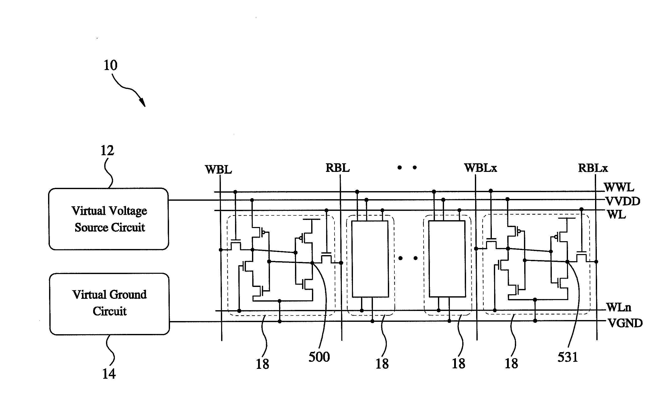
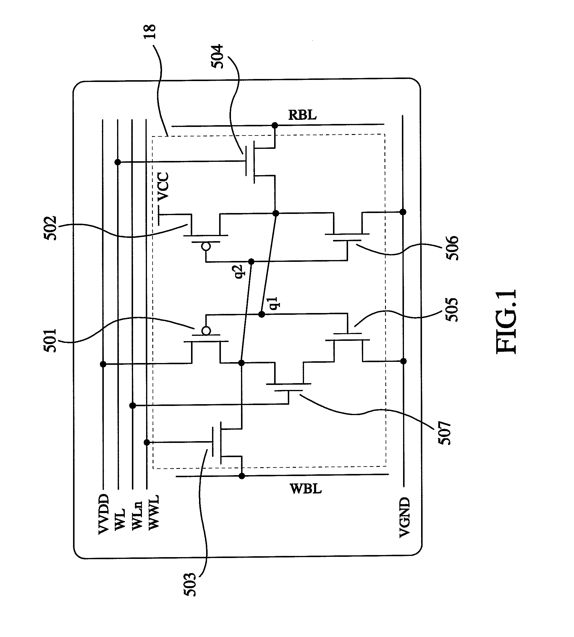
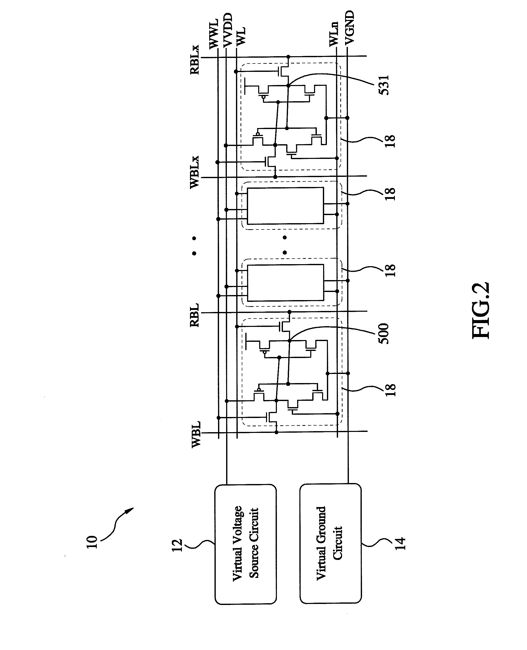
[0040]Referring to FIGS. 1-4, a memory circuit 10 properly workable under low working voltage in accordance with a preferred embodiment of the present invention is composed of a plurality of write word lines WWL, a plurality of write bit lines WBL, a plurality of read / write word lines WL, a plurality of read / write bit lines RBL, a plurality of read / write inverted word lines WLn, a plurality of virtual voltage source circuits 12, a plurality of virtual ground circuits 14, and a plurality of asymmetrical RAM cells 18. The detailed descriptions and operations of these elements as well as their interrelations are recited in the respective paragraphs as follows.

[0041]The asymmetrical RAM cells 18 constitutes a cell array (not shown), which is connected with the write word lines WWL, the write bit lines WBL, the read / write word lines WL, the read / write bit lines RBL, the read / write inverted word lines WLn, the virtual voltage source circuits 12, and the virtual ground circuits 14. It is d...


PUM


Abstract

A memory circuit properly workable under low working voltage includes a plurality of write word lines, a plurality of write bit lines, a plurality of read/write word lines, a plurality of read/write bit lines, a plurality of read/write inverted word lines, a plurality of virtual voltage source circuits, a plurality of virtual ground circuits, and a plurality of asymmetrical RAM cells constituting a cell array. The asymmetrical RAM cells are formed of seven transistors, five of which are NMOS transistors and two of which are PMOS transistors. The virtual voltage power source circuit and the virtual ground circuit can reinforce the write-in and read abilities under low working voltage to make the write-in and read actions more stable, decrease leakage current, and lower power consumption.

Description

BACKGROUND OF THE INVENTION[0001]1. Field of the Invention[0002]The present invention relates generally to the architecture of memory cells in the integrated circuit (IC), and more particularly, to a memory circuit properly workable under low working voltage.[0003]2. Description of the Related Art[0004]The area and power of the static random access memory (SRAM) are key challenges for very large scale IC or system on chip; if the area is smaller, the cost of the chip can be reduced more effectively and the reliability of the memory circuit can be enhanced. Besides, the low-voltage operation has become one of the trends of the current low-power IC design, so the design of SRAM also needs to be developed toward low voltage and should take noise immunocompetence into account.[0005]Among the rough classifications of SRAM cells, the conventional six-transistor (6T) cell is the most typical example. Thereafter, the SRAM cell was developed to be 7T cell, 8T cell, and 10T cell to properly w...

Claims


Application Information

Patent Timeline
IPC IPC(8): G11C11/40
CPCG11C11/412G11C11/419
Inventor WANG, JINN-SHYANCHANG, PEI-YAO
Owner NATIONAL CHUNG CHENG UNIV
Why Eureka
Try Eureka