Dual damascene dual alignment interconnect scheme

a dual-alignment, interconnect technology, applied in the direction of electrical equipment, semiconductor devices, semiconductor/solid-state device details, etc., can solve the problems of reliability failure of semiconductor chips, overextension of conventional dual-alignment methods,

Inactive Publication Date: 2013-12-12
ALSEPHINA INNOVATIONS INC
View PDF4 Cites 62 Cited by
  • Summary
  • Abstract
  • Description
  • Claims
  • Application Information

AI Technical Summary

Problems solved by technology

Conventional dual damascene methods do not provide a mechanism to systematically prevent overextension of a via structure to an adjacent underlying metal line.
Thus, overlay issues du

Method used


Image

  • Dual damascene dual alignment interconnect scheme
  • Dual damascene dual alignment interconnect scheme
  • Dual damascene dual alignment interconnect scheme

Examples


Embodiment Construction

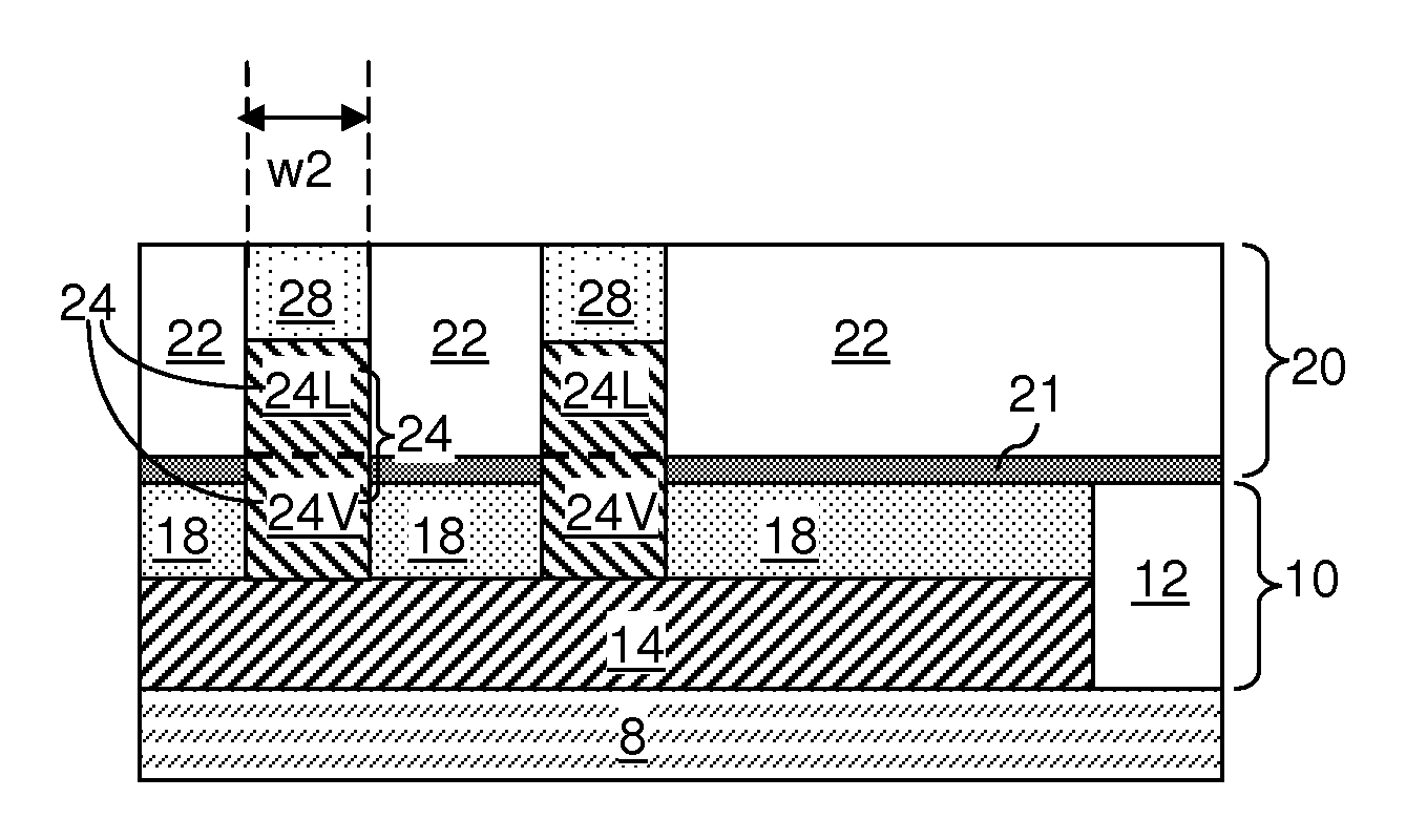
[0040]As stated above, the present disclosure relates to a metal interconnect structure that includes an integrated line and via structure in which the via structure is self-aligned in two independent horizontal directions, and methods of manufacturing the same. Aspects of the present disclosure are now described in detail with accompanying figures. It is noted that like and corresponding elements are referred to by like reference numerals. The drawings are not drawn to scale.

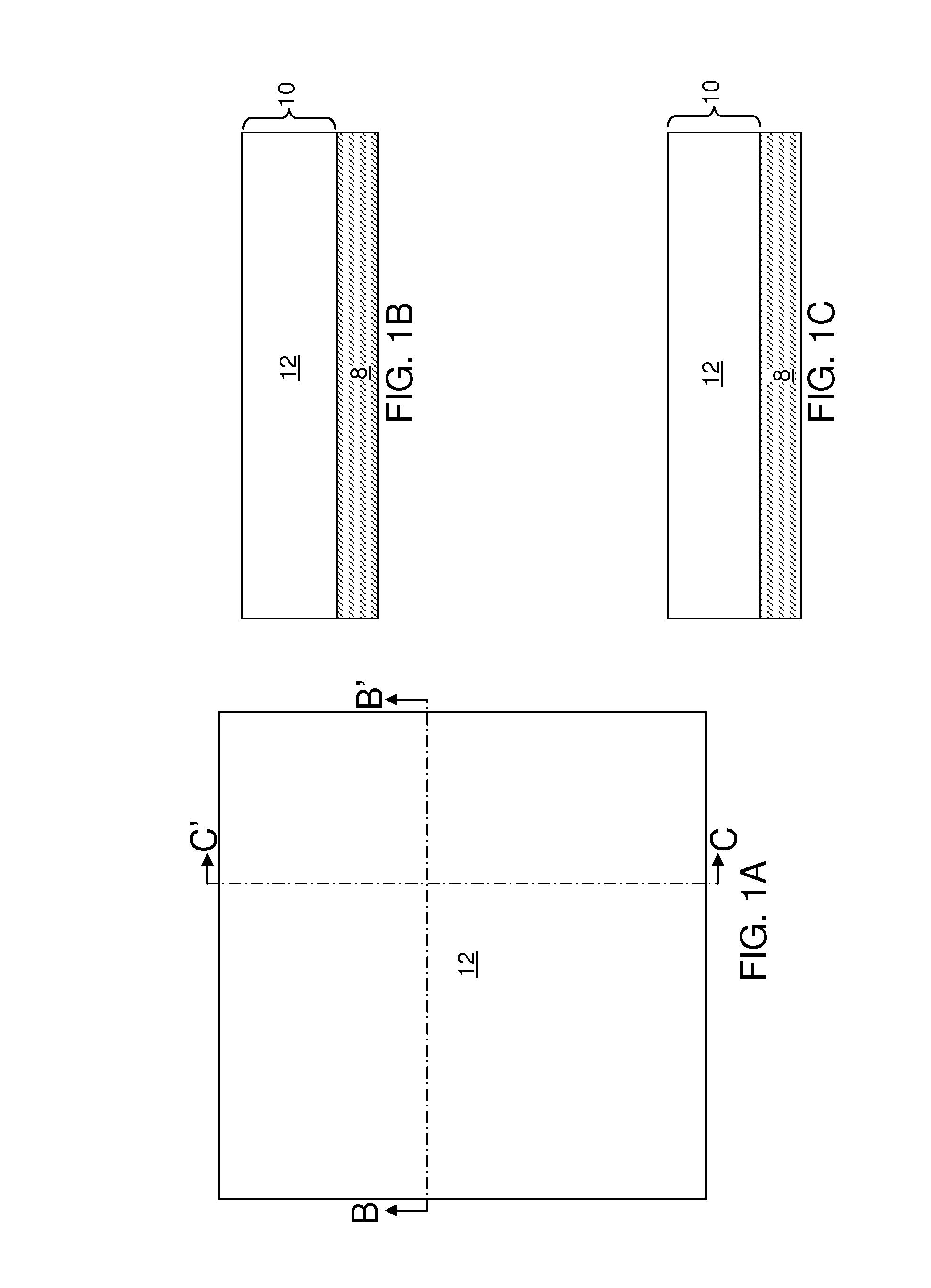
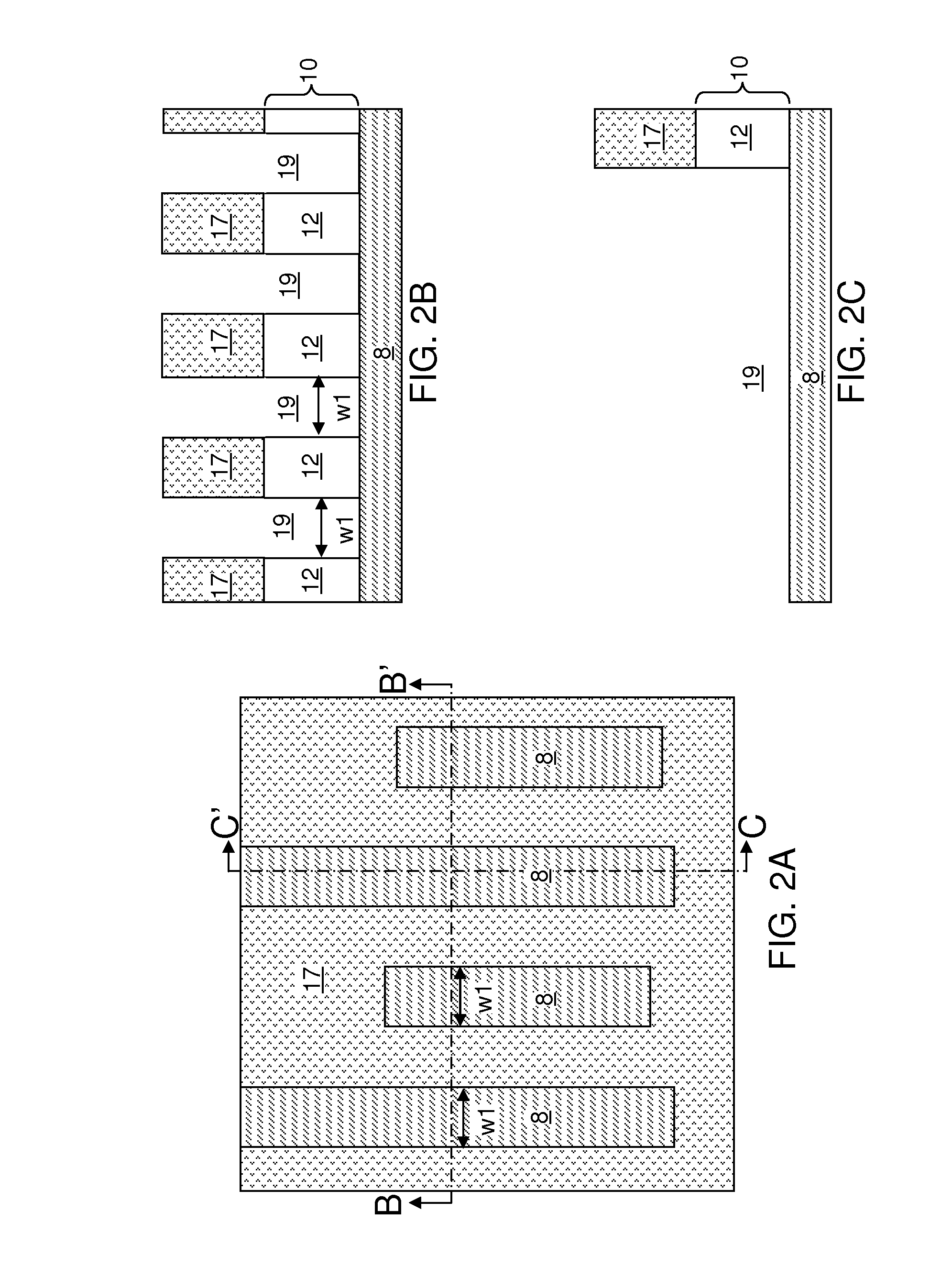
[0041]Referring to FIGS. 1A, 1B, and 1C, an exemplary metal interconnect structure according to an embodiment of the present disclosure can be formed by providing a substrate 8, and depositing a first dielectric material layer 12 on a top surface of the substrate 8. The substrate 8 can be a semiconductor substrate having at least one semiconductor device thereupon and / or therein, or can be a stack of a semiconductor substrate and at least one underlying metal interconnect structure that includes at least one co...


PUM


Abstract

A stack of a first metal line and a first dielectric cap material portion is formed within a line trench of first dielectric material layer. A second dielectric material layer is formed thereafter. A line trench extending between the top surface and the bottom surface of the second dielectric material layer is patterned. A photoresist layer is applied over the second dielectric material layer and patterned with a via pattern. An underlying portion of the first dielectric cap material is removed by an etch selective to the dielectric materials of the first and second dielectric material layer to form a via cavity that is laterally confined along the widthwise direction of the line trench and along the widthwise direction of the first metal line. A dual damascene line and via structure is formed, which includes a via structure that is laterally confined along two independent horizontal directions.

Description

BACKGROUND[0001]The present disclosure relates to a metal interconnect structure, and particularly to a metal interconnect structure that includes an integrated line and via structure in which the via structure is self-aligned in two independent horizontal directions, and methods of manufacturing the same.[0002]Alignment of a via structure to an underlying metal line is important in order to prevent yield degradation due to undesired electrical opens or undesired electrical shorts that are detected during testing, or reliability issues that arise during the operation of a semiconductor chip due to degradation of electrical contacts. Conventional dual damascene methods do not provide a mechanism to systematically prevent overextension of a via structure to an adjacent underlying metal line. Thus, overlay issues during lithographic patterning of via cavities can result in immediate or potential electrical shorts, and depress the yield and / or cause a reliability failure of a semiconduc...

Claims


Application Information

Patent Timeline
IPC IPC(8): H01L23/48H01L21/28
CPCH01L21/76897H01L21/76807H01L21/76808H01L21/76811H01L21/76819H01L21/76831H01L21/76832H01L21/76834H01L21/76883H01L23/5226H01L2924/0002
Inventor HOLMES, STEVEN J.HORAK, DAVID V.KOBURGER, III, CHARLES W.PONOTH, SHOMYANG, CHIH-CHAO
Owner ALSEPHINA INNOVATIONS INC
Why Eureka
Try Eureka