Wafer processing method

a processing method and wafer technology, applied in the field of wafer processing methods, can solve the problems of faulty suction holding of the wafer, no chamfering of the sic wafer, damage to the device formed on the front side, etc., and achieve the effect of preventing the damage of the device and the faulty suction holding

Inactive Publication Date: 2013-12-26
SEKIYA KAZUMA
View PDF9 Cites 5 Cited by
  • Summary
  • Abstract
  • Description
  • Claims
  • Application Information

AI Technical Summary

Benefits of technology

[0008]It is therefore an object of the present invention to provide a wafer processing method which can prevent the damage to the devices and the faulty suction holding of the wafer in the subsequent step due to the ridge portion of the epitaxial film, regardless of the kind of the wafer.
[0011]According to the present invention, the ridge portion (edge crown) formed along the peripheral edge of the wafer having the epitaxial film formed on the front side is removed by grinding. Accordingly, it is possible to prevent the damage to the devices and the faulty suction holding of the wafer in the subsequent step due to the ridge portion of the epitaxial film.

Problems solved by technology

However, there is a case that the chamfered portion is small or no chamfering is performed depending on the kind of the wafer.
There is a possibility that the edge crown (ridge portion of the epitaxial film) formed on the front side of the wafer along the peripheral edge thereof may be broken during transportation of the wafer to cause damage to the devices formed on the front side of the wafer.
Further, when an edge crown is formed on the back side of the wafer, there is a possibility that faulty suction holding of the wafer may occur in holding the back side of the wafer under suction in a subsequent step.
However, there is a case that no chamfering is performed on an SiC wafer.
When an epitaxial film is formed on the SiC wafer by epitaxial growth, edge crowns are formed on the front side and back side of the wafer along the peripheral edge thereof, causing the damage to the devices formed on the front side of the wafer or the faulty suction holding of the wafer in the subsequent step.

Method used


Image

  • Wafer processing method
  • Wafer processing method
  • Wafer processing method

Examples


Embodiment Construction

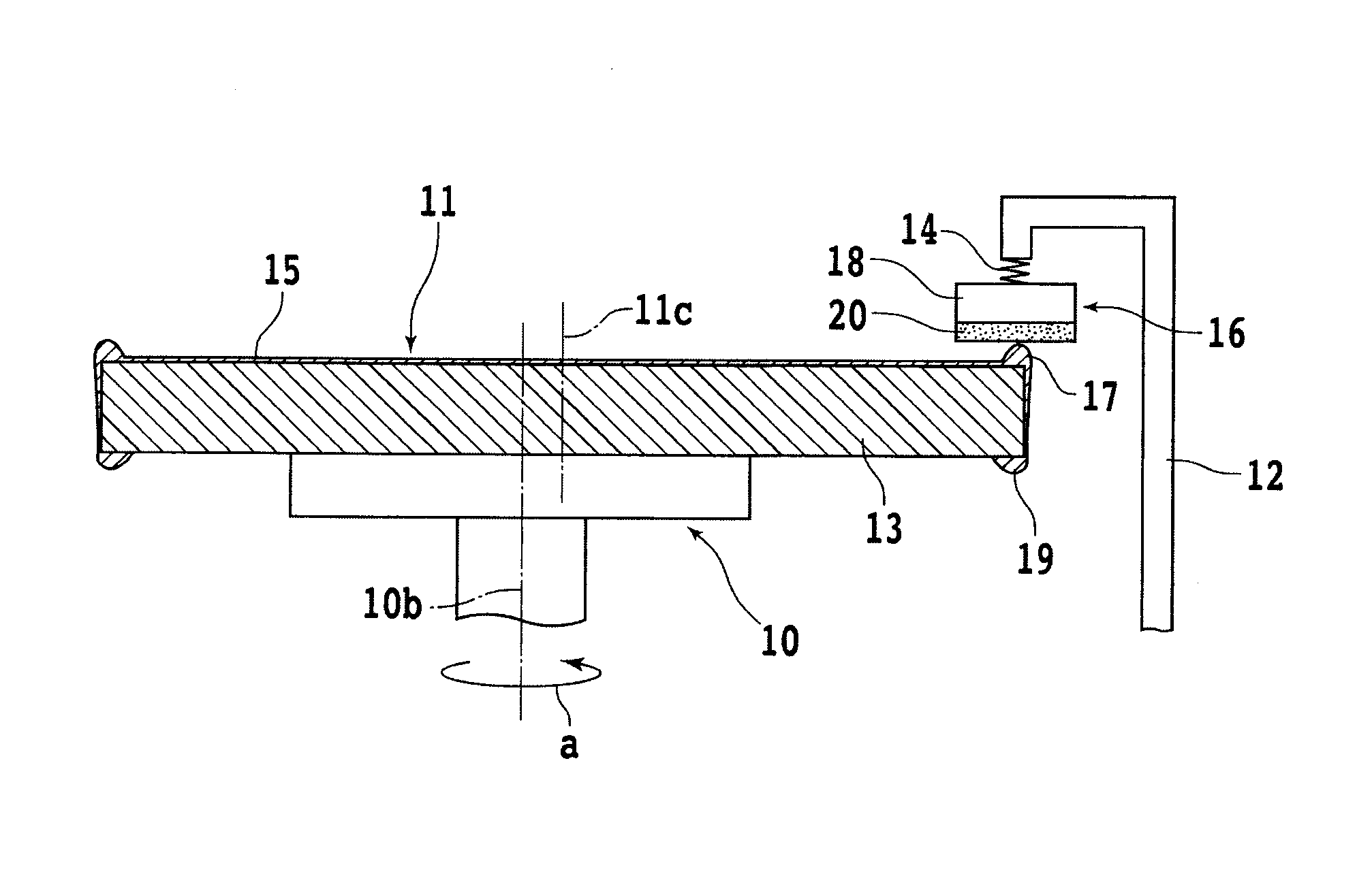
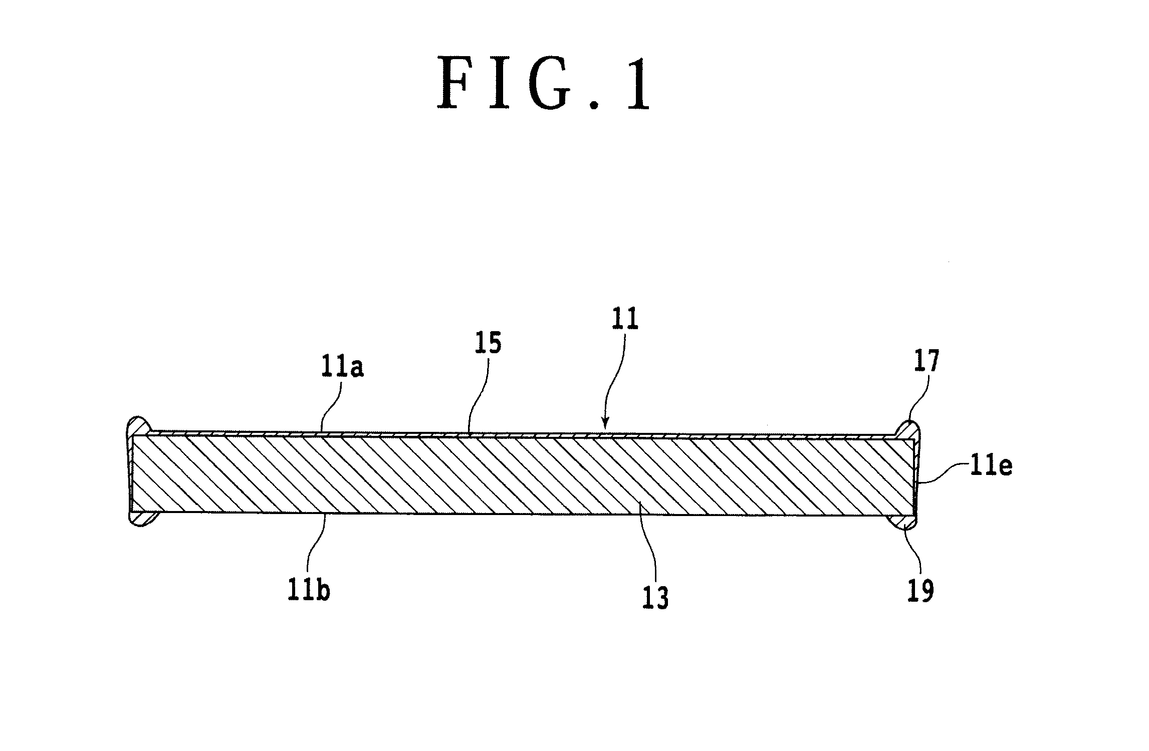
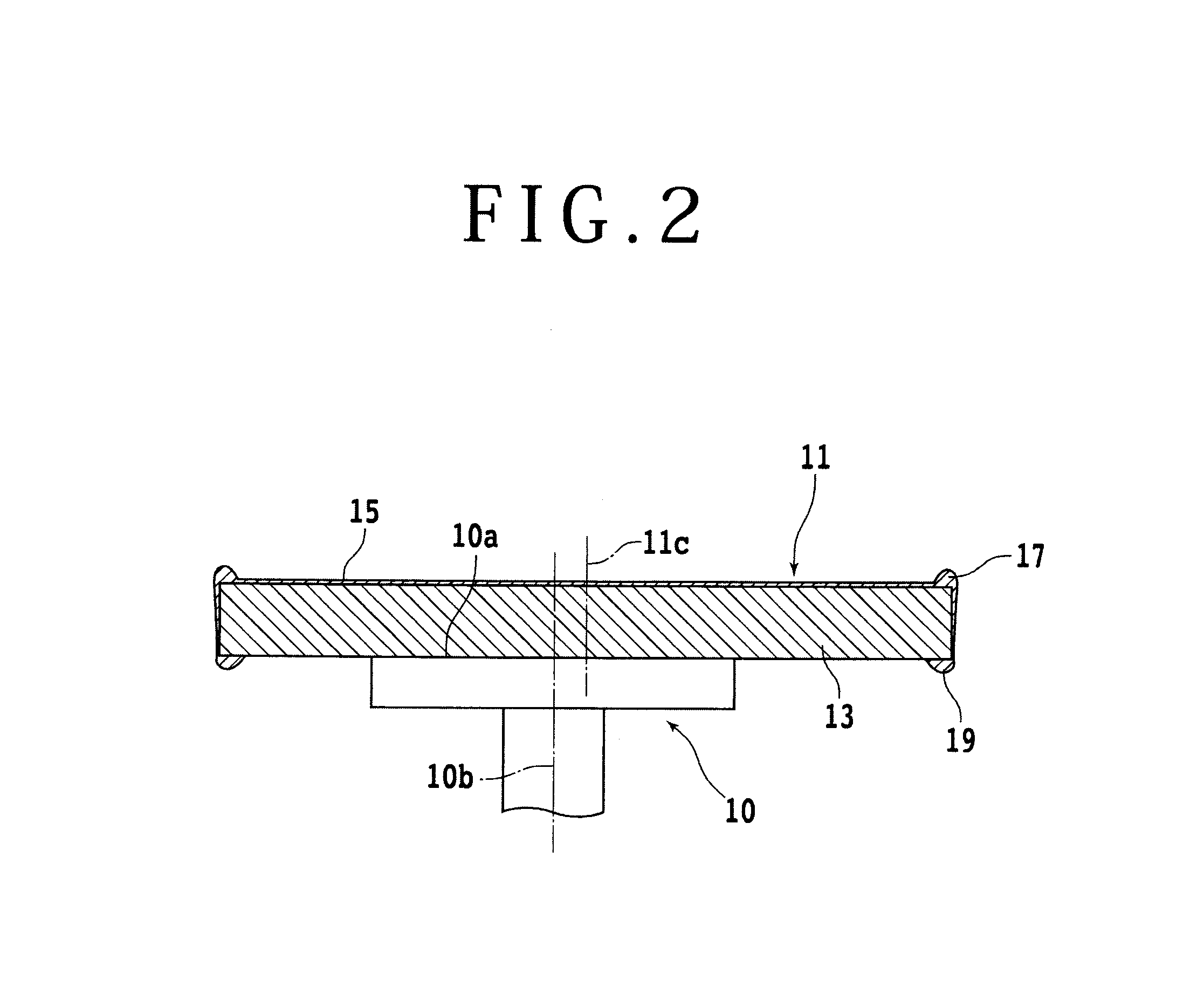
[0017]A preferred embodiment of the present invention will now be described in detail with reference to the drawings. Referring to FIG. 1, there is shown an SiC (silicon carbide) wafer 11. The SiC wafer 11 is composed of an SiC bulk wafer (SiC substrate) 13 and an epitaxial film 15 formed on the SiC bulk wafer 13 by epitaxial growth. That is, the epitaxial film 15 is formed as a single-crystal SiC thin film. Usually, the epitaxial film 15 of the SiC wafer 11 is formed by CVD (Chemical Vapor Deposition) or the like. The SiC wafer 11 has a front side 11a (upper surface), a back side 11b (lower surface), and a peripheral surface 11e substantially perpendicular to both the front side 11a and the back side 11b. That is, the peripheral surface 11e of the SiC wafer 11 is not formed with a chamfered portion.

[0018]In the case that the epitaxial film 15 is formed by epitaxial growth on such a wafer having no chamfered portion, e.g., the SiC wafer 11 as mentioned above, edge crowns (ridge port...


PUM

PropertyMeasurementUnit
thicknessaaaaaaaaaa
semiconductoraaaaaaaaaa
heightaaaaaaaaaa

Abstract

A wafer processing method of processing a wafer having an epitaxial film formed on the front side. The wafer processing method includes a holding step of holding the wafer on a holding table having a holding surface for holding the wafer and a rotational axis extending perpendicularly to the holding surface and passing through the center of the holding surface, and a removing step of pressing a grinding member on a ridge portion formed along the peripheral edge of the wafer held on the holding table and rotating the holding table about the rotational axis, thereby removing the ridge portion.

Description

BACKGROUND OF THE INVENTION[0001]1. Field of the Invention[0002]The present invention relates to a wafer processing method of processing a wafer having an epitaxial film formed on the front side.[0003]2. Description of the Related Art[0004]Epitaxial growth on the front side of a semiconductor crystal substrate (wafer) of silicon (Si) or the like causes undesirable formation of a ridge portion of an epitaxial film, called edge crown, along the peripheral edge of the wafer. To cope with this problem, the peripheral edge of the wafer is generally formed with a chamfered portion to suppress the occurrence of abnormal growth in the epitaxial growth, i.e., the formation of the edge crown and to also prevent the occurrence of cracking or chipping due to the contact of the peripheral edge of the wafer in handling or transporting the wafer.[0005]However, when the epitaxial film has a large thickness, the height of the edge crown is increased to more than 10 μm in some cases. In such a wafer,...

Claims


Application Information

Patent Timeline
Patent Type & Authority Applications(United States)
IPC IPC(8): B24B9/06
CPCB24B9/065H01L21/304H01L29/1608
Inventor SEKIYA, KAZUMA
Owner SEKIYA KAZUMA
Why Eureka
Try Eureka