
Liquid crystal display device

a liquid crystal display and display device technology, applied in non-linear optics, instruments, optics, etc., can solve the problems of low production yield, low reliability, serious problems, etc., and achieve the effect of low production cost, high reliability and high production yield

Active Publication Date: 2014-01-09
PANASONIC INTELLECTUAL PROPERTY CORP OF AMERICA
View PDF0 Cites 0 Cited by
  • Summary
  • Abstract
  • Description
  • Claims
  • Application Information

AI Technical Summary

Benefits of technology

This patent aims to improve the production efficiency and reliability of IPS liquid crystal display devices by using a smaller number of layers to reduce production costs. The invention achieves this by not dissolving the source, drain, or image signal line in the developer when patterning the ITO to form the pixel electrode. This results in a higher yield of devices and increased reliability. Additionally, this invention allows for the creation of an IPS liquid crystal display device with fewer layers, reducing production expenses.

Problems solved by technology

In the case of the liquid crystal display device, viewing angle characteristics are a problem.
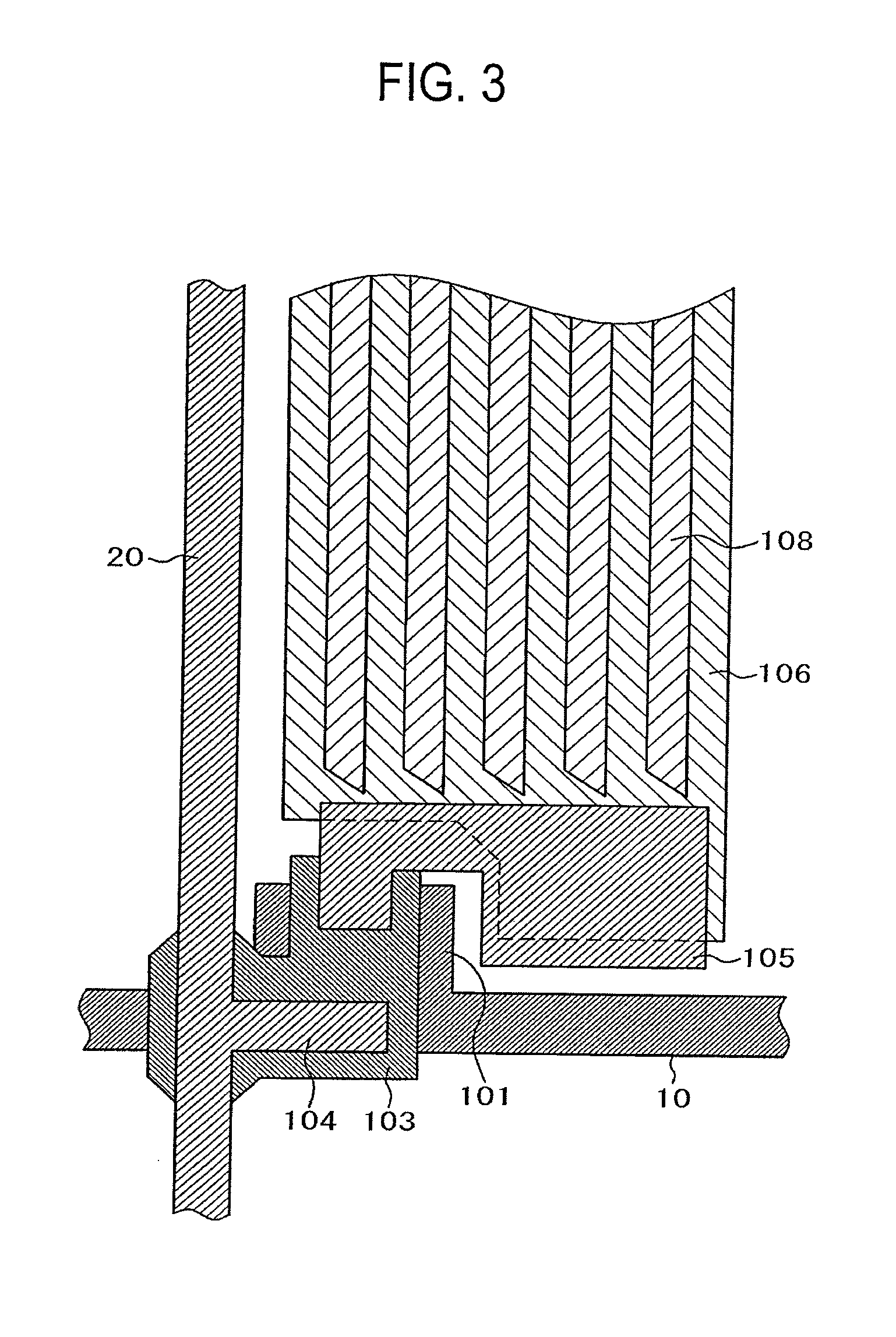
In particular, this problem is serious in the image signal line 20 because it is narrow and long.
This leads to the risk of a low production yield as well as a low reliability.

Method used


Image

  • Liquid crystal display device
  • Liquid crystal display device
  • Liquid crystal display device

Examples


first embodiment

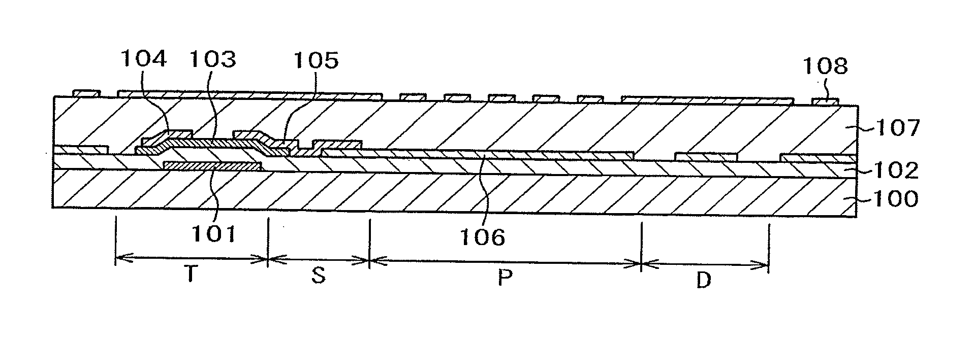
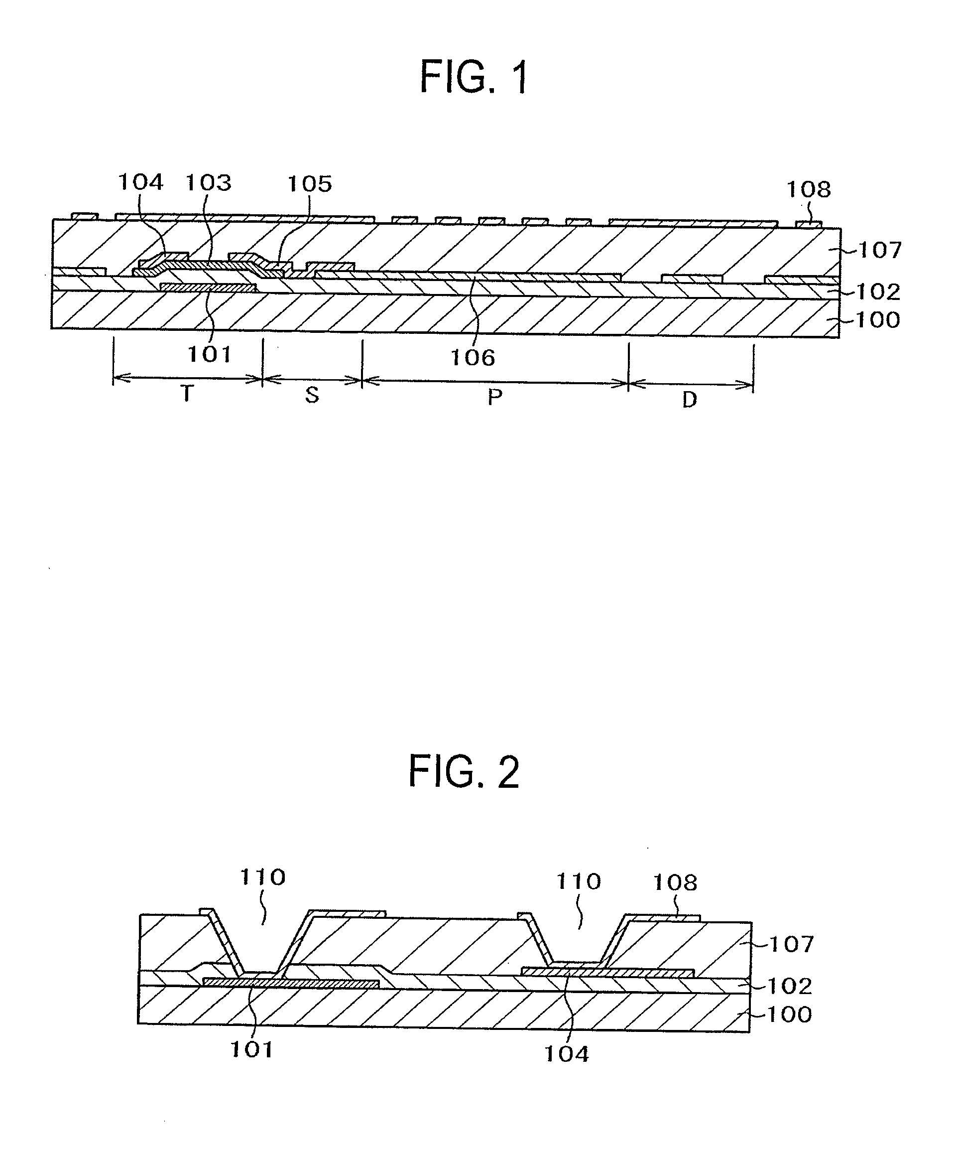
[0032]FIG. 1 is a cross-sectional view of a TFT substrate 100 according to a first embodiment of the present invention. In FIG. 1, the configuration is the same as the configuration described above with reference to FIG. 5, except for the order of laminating a pixel electrode 106 and a source electrode 105. Thus, the repeated description will be omitted. In FIG. 1, a gate electrode 101 has a two-layer structure, in which the lower layer is formed from AlNd alloy 200 nm thick, and the upper layer is formed from MoCr alloy 40 nm thick. The two-layer structure serves to prevent the ITO laminated on the terminal portion from reacting with AlNd when a terminal portion, which will be described below, is formed on the same layer as the gate electrode 101.

[0033]On the gate electrode 101, a gate insulating film 102 is formed with a thickness of about 350 nm by CVD. Then, an a-Si film, which is the semiconductor layer 103, is formed with a thickness of about 150 nm by CVD on the gate insulati...


PUM


Abstract

In a liquid crystal display which includes a liquid crystal layer between a TFT substrate and a counter substrate, a gate electrode, a gate insulator and a semiconductor layer are laminated. A pixel electrode is formed on the gate insulator and metal source and drain electrodes are formed on the semiconductor layer and gate insulator. At least upper surfaces of the source and drain electrode contain Mo. One of the source and drain electrodes is directly laminated on a portion of the pixel electrode, which portion is disposed on the gate insulating film.

Description

CROSS-REFERENCE TO RELATED APPLICATIONS[0001]This application is a continuation application of U.S. application Ser. No. 13 / 229,782, filed Sep. 12, 2011, the entire contents of which are incorporated herein by reference.CLAIM OF PRIORITY[0002]The present application claims priority from Japanese Patent Application JP 2010-217062 filed on Sep. 28, 2010, the content of which is hereby incorporated by reference into this application.FIELD OF THE INVENTION[0003]The present invention relates to a display device, and more particularly, to a liquid crystal display device of lateral electric field mode that can achieve excellent viewing angle characteristics and reduce the production cost.BACKGROUND OF THE INVENTION[0004]A liquid crystal display panel used in a liquid crystal display device includes a TFT substrate in which pixels each having a pixel electrode, a thin film transistor (TFT), and the like, are arranged in a matrix form. A counter substrate is disposed opposite to the TFT subs...

Claims


Application Information

Patent Timeline
Patent Type & Authority Applications(United States)
IPC IPC(8): G02F1/1368
CPCG02F1/1368G02F1/134363G02F1/13458G02F1/136286G02F1/134318G02F1/136231G02F1/13629G02F1/1343G02F1/134336G02F1/134372
Inventor ANJO, KENJIOOTANI, TOMOHIKO
Owner PANASONIC INTELLECTUAL PROPERTY CORP OF AMERICA
Learn More