
Electronic device and manufacturing method thereof

a manufacturing method and electronic device technology, applied in the direction of sustainable manufacturing/processing, printed circuit non-printed electric component association, final product manufacturing, etc., can solve the problem that the conductive lines made by the general semiconductor thin-film process cannot be directly used to electrically connect the electronic element to the circuit substrate, and achieve the effect of improving the production yield and reliability reducing the manufacturing cost of the electronic device, and increasing the configuration density of the componen

Active Publication Date: 2020-05-12
GIO OPTOELECTRONICS CORP
View PDF10 Cites 1 Cited by
  • Summary
  • Abstract
  • Description
  • Claims
  • Application Information

AI Technical Summary

Benefits of technology

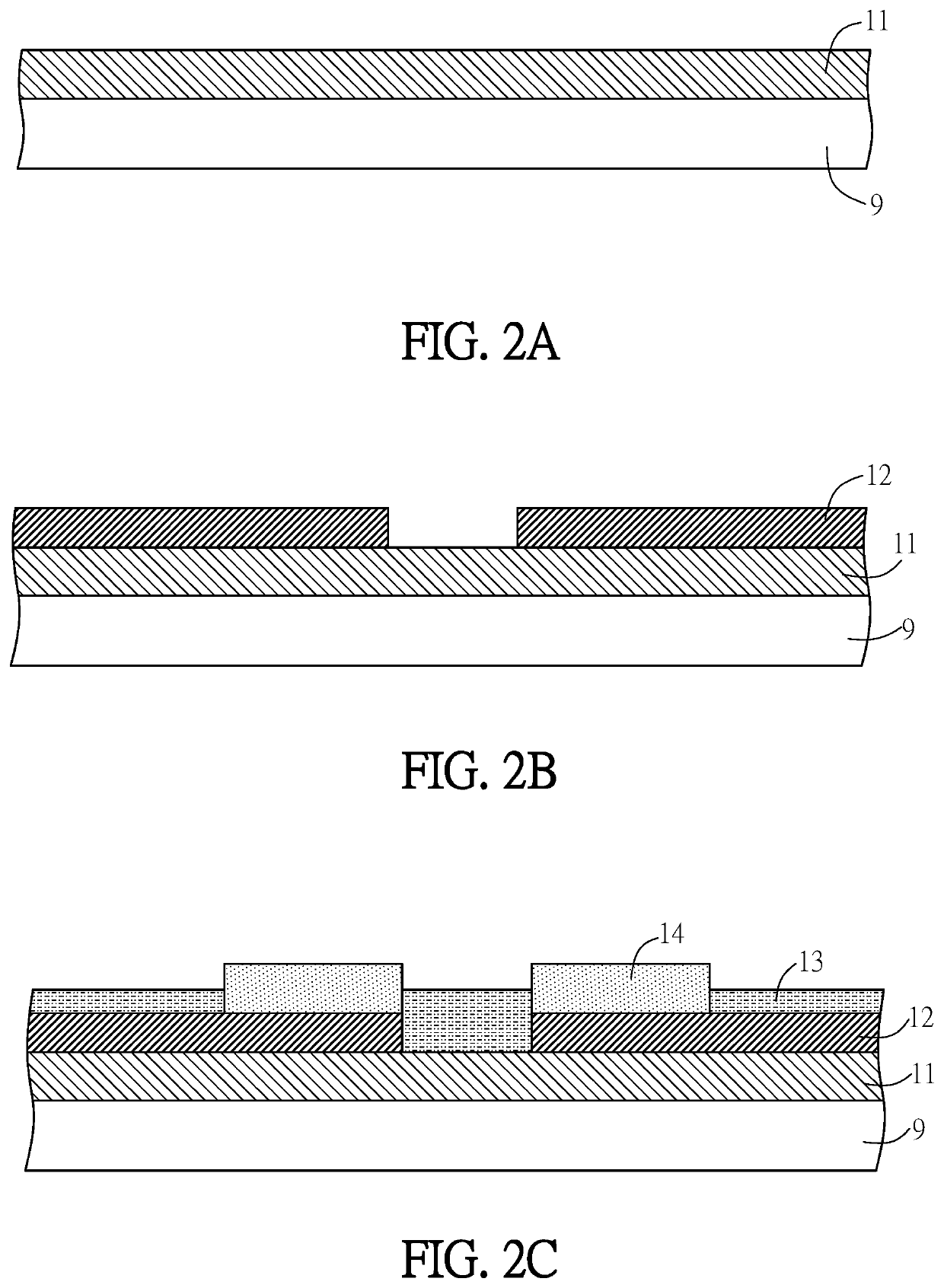
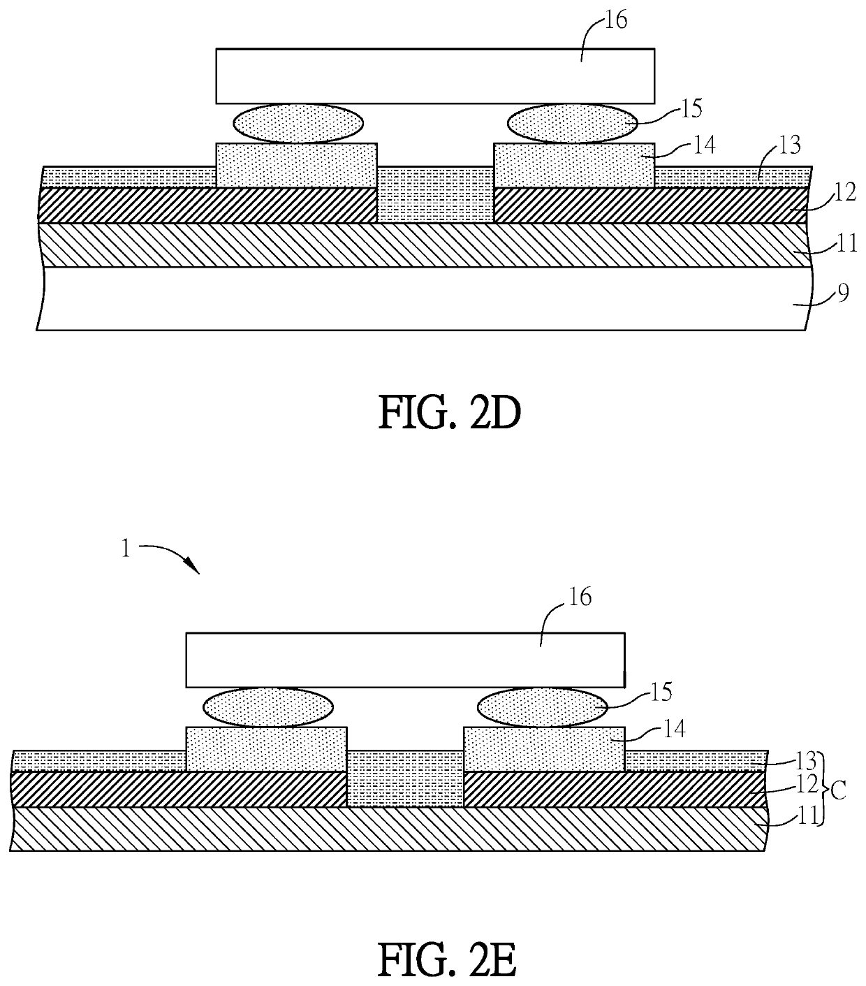
[0026]As mentioned above, in the electronic device and the manufacturing method thereof of this disclosure, at least a thin-film conductive line is formed on the substrate by a thin-film process, and at least an electrical connection pad electrically connected with the thin-film conductive line is formed on the substrate by a printing process. Afterwards, at least an electronic element is disposed on the substrate, and the electronic element can be electrically connected with the thin-film conductive line via the electrical connection pad. Since thin-film conductive line and the electrical connection pad are formed on the substrate by a thin-film process and a printing process, respectively, and the electronic element is electrically connected with the thin-film conductive line via the electrical connection pad, many fine lines can be manufactured based on this disclosure. Accordingly, this disclosure can decrease the manufacturing cost of the electronic device, increase the component configuration density, and improve the production yield and reliability of the electronic device.

Problems solved by technology

Accordingly, the conductive lines made by the general semiconductor thin-film process cannot be directly used for electrically connecting the electronic element to the circuit substrate.

Method used


Image

  • Electronic device and manufacturing method thereof
  • Electronic device and manufacturing method thereof
  • Electronic device and manufacturing method thereof

Examples


Embodiment Construction

[0031]The present disclosure will be apparent from the following detailed description, which proceeds with reference to the accompanying drawings, wherein the same references relate to the same elements.

[0032]For example, the electronic device in the following embodiments can be an LED display, a micro-LED display, a sensing device (e.g. fingerprint sensor, fingerprint reader, or an X-ray sensor), a semiconductor device, or an illumination device, and this disclosure is not limited thereto.

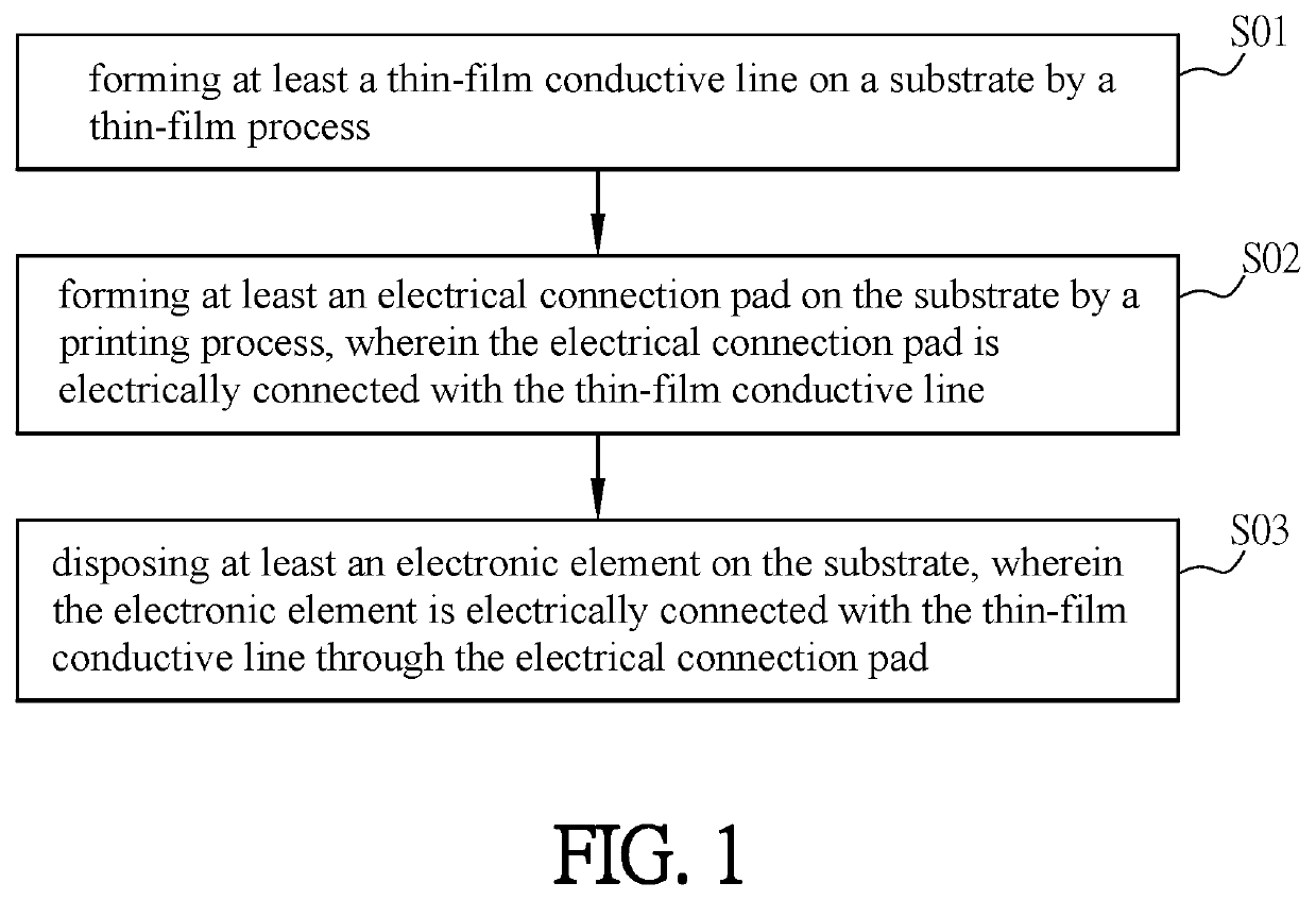
[0033]FIG. 1 is a flow chart showing a manufacturing method of an electronic device according to an embodiment of this disclosure.

[0034]As shown in FIG. 1, the manufacturing method of an electronic device comprises the following steps of: forming at least a thin-film conductive line on a substrate by a thin-film process (step S01); forming at least an electrical connection pad on the substrate by a printing process, wherein the electrical connection pad is electrically connected with the thin-film...


PUM

PropertyMeasurementUnit
porosityaaaaaaaaaa
thicknessaaaaaaaaaa
thicknessaaaaaaaaaa

Abstract

An electronic device and manufacturing method thereof are disclosed. The manufacturing method of the electronic device comprises following steps: forming at least a thin-film conductive line on the substrate by a thin-film process; forming at least an electrical connection pad on the substrate by a printing process, wherein the electrical connection pad is electrically connected with the thin-film conductive line; and disposing at least an electronic element on the substrate, wherein the electronic element is electrically connected with the thin-film conductive line through the electrical connection pad. The electronic device has a lower manufacturing cost and a higher component configuration density, and the production yield and reliability of the electronic device are improved by the configuration of the electrical connection pad.

Description

CROSS REFERENCE TO RELATED APPLICATIONS[0001]This Non-provisional application claims priority under 35 U.S.C. § 119(a) on Patent Application No(s). 106136523 filed in Taiwan, Republic of China on Oct. 24, 2017, the entire contents of which are hereby incorporated by reference.BACKGROUNDTechnology Field[0002]The present disclosure relates to an electronic device and, in particular, to an electronic device and a manufacturing method thereof.Description of Related Art[0003]In the conventional manufacturing process of the semiconductor electronic device (e.g. an LED display), the conductive lines disposed on the circuit substrate must be made with a certain thickness (generally greater than 3 μm) for connecting the circuit substrate to an electronic element. However, the conductive lines made by the general semiconductor thin-film process usually have a thinner thickness (generally less than 3 μm). Accordingly, the conductive lines made by the general semiconductor thin-film process can...

Claims


Application Information

Patent Timeline
Patent Type & Authority Patents(United States)
IPC IPC(8): H05K1/18H05K1/11H05K3/32H05K3/40H05K3/00H05K1/03
CPCH05K1/118H05K3/4076H05K1/189H05K1/111H05K3/321H05K3/32H05K2201/0179H05K3/007H05K2201/0373H01L2224/16225H05K1/0313H05K2201/0338H05K2203/0353Y02P70/50H01L2224/81193H01L2224/81805H01L2224/16238H01L2224/16227H01L24/16H01L24/81
Inventor LI, CHIN-TANG
Owner GIO OPTOELECTRONICS CORP
Learn More