
Thermally enhanced semiconductor assembly with heat spreader and integrated dual build-up circuitries and method of making the same

a technology of heat spreader and semiconductor assembly, which is applied in the direction of semiconductor devices, semiconductor/solid-state device details, electrical apparatus, etc., can solve the problems of performance degradation, many performance-related deficiencies, and significant thermal, electrical, form-factor and reliability challenges of the semiconductor packaging industry

Inactive Publication Date: 2017-02-14
BRIDGE SEMICON
View PDF11 Cites 0 Cited by
  • Summary
  • Abstract
  • Description
  • Claims
  • Application Information

AI Technical Summary

Benefits of technology

This patent describes a semiconductor assembly with improved production yield and reliability. It achieves this by using a heat spreader to dissipate the heat generated by the semiconductor device and improve its signal integrity. The assembly includes two build-up circuitries integrated together for high routing flexibility and the shortest possible interconnection length. The semiconductor device is also enclosed in a heat spreader for better heat dissipation. The method of making the assembly ensures good electrical connection and prevents contact pad disconnection problems. Overall, this patent provides a solution for improving the performance and reliability of semiconductor assemblies.

Problems solved by technology

The convergence of mobility, communication, and computing has created significant thermal, electrical, form-factor and reliability challenges to the semiconductor packaging industry.
Despite numerous configurations for embedding semiconductor chip in wiring board or mold compound reported in the literature, many performance-related deficiencies remain.
For example, the assemblies disclosed by U.S. Pat. Nos. 8,742,589, 8,735,222, 8,679,963, 8,453,323 may render performance degradation problems as the heat generated by the embedded chip can't be dissipated properly through the thermally insulating material such as laminate or mold compound.
Further, as these assemblies utilize micro-vias for electrical connection of the embedded chip, a significant drawback arising from the fabrication of the above assembly structures is that the embedded chip may dislocate during encapsulation or lamination process.
Incomplete metallization of micro-via on the chip I / O pad due to chip dislocation as described in U.S. Pat. Nos. 8,501,544, 7,935,893 further degrades the quality of the electrical connection, thereby lowering reliability and production yield of the fabricated assembly.

Method used


Image

  • Thermally enhanced semiconductor assembly with heat spreader and integrated dual build-up circuitries and method of making the same
  • Thermally enhanced semiconductor assembly with heat spreader and integrated dual build-up circuitries and method of making the same
  • Thermally enhanced semiconductor assembly with heat spreader and integrated dual build-up circuitries and method of making the same

Examples


embodiment 1

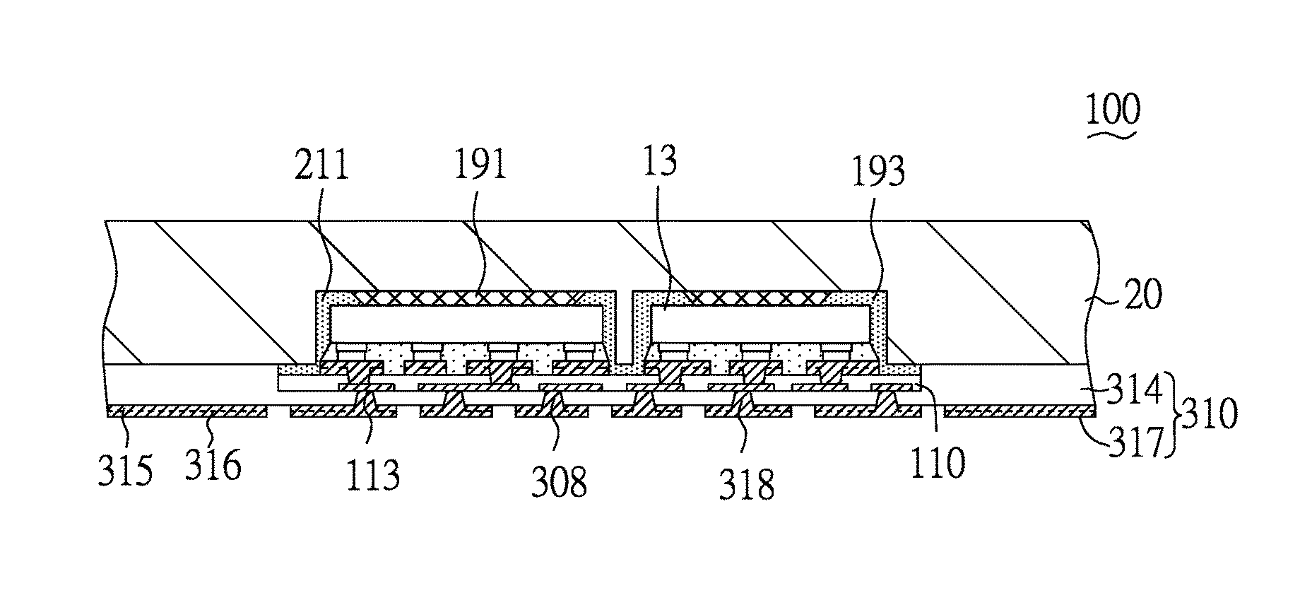
[0059]FIGS. 1-26 are schematic views showing a method of making a semiconductor assembly that includes semiconductor devices 13, a heat spreader 20, a first build-up circuitry 110 and a second build-up circuitry 310 in accordance with an embodiment of the present invention.

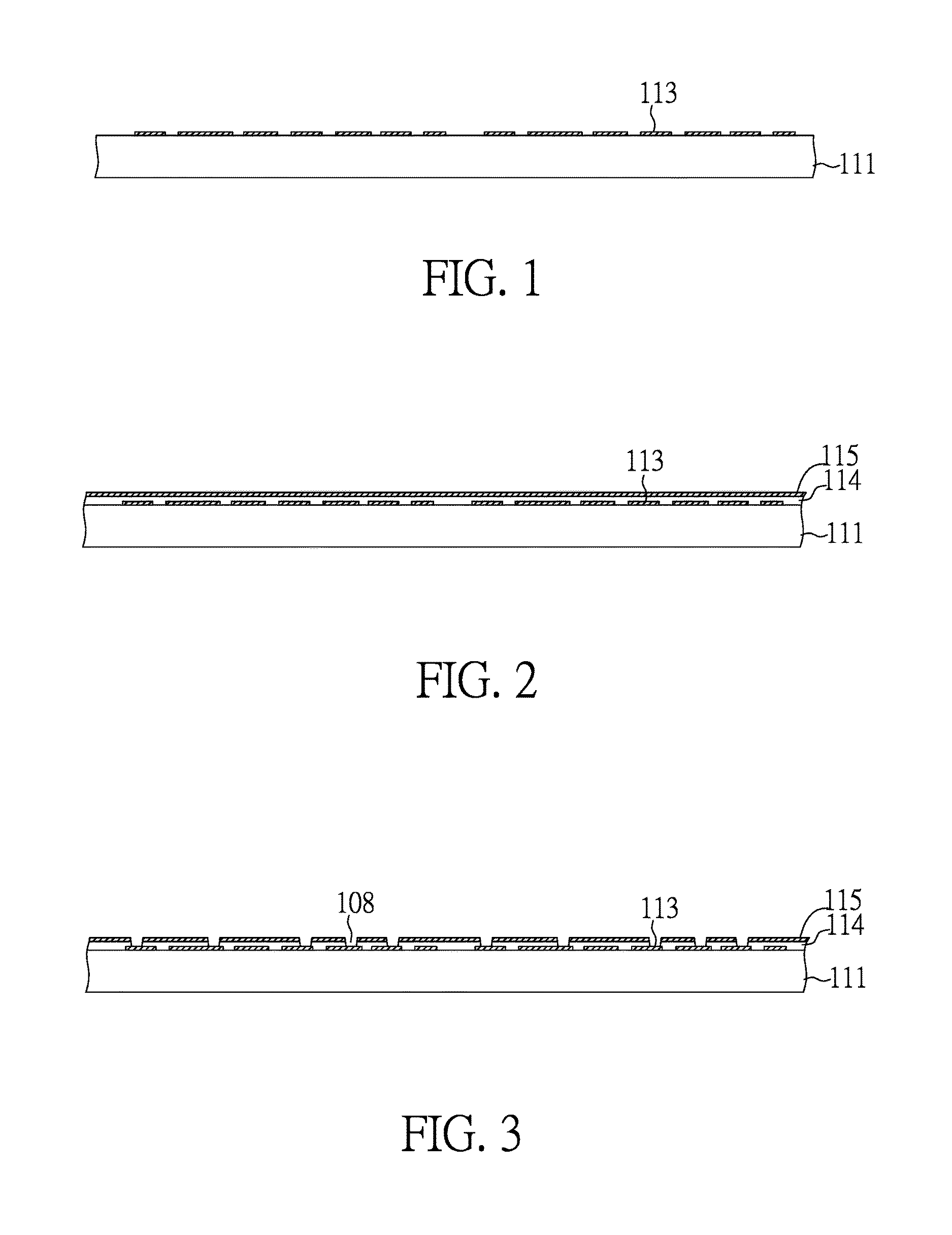
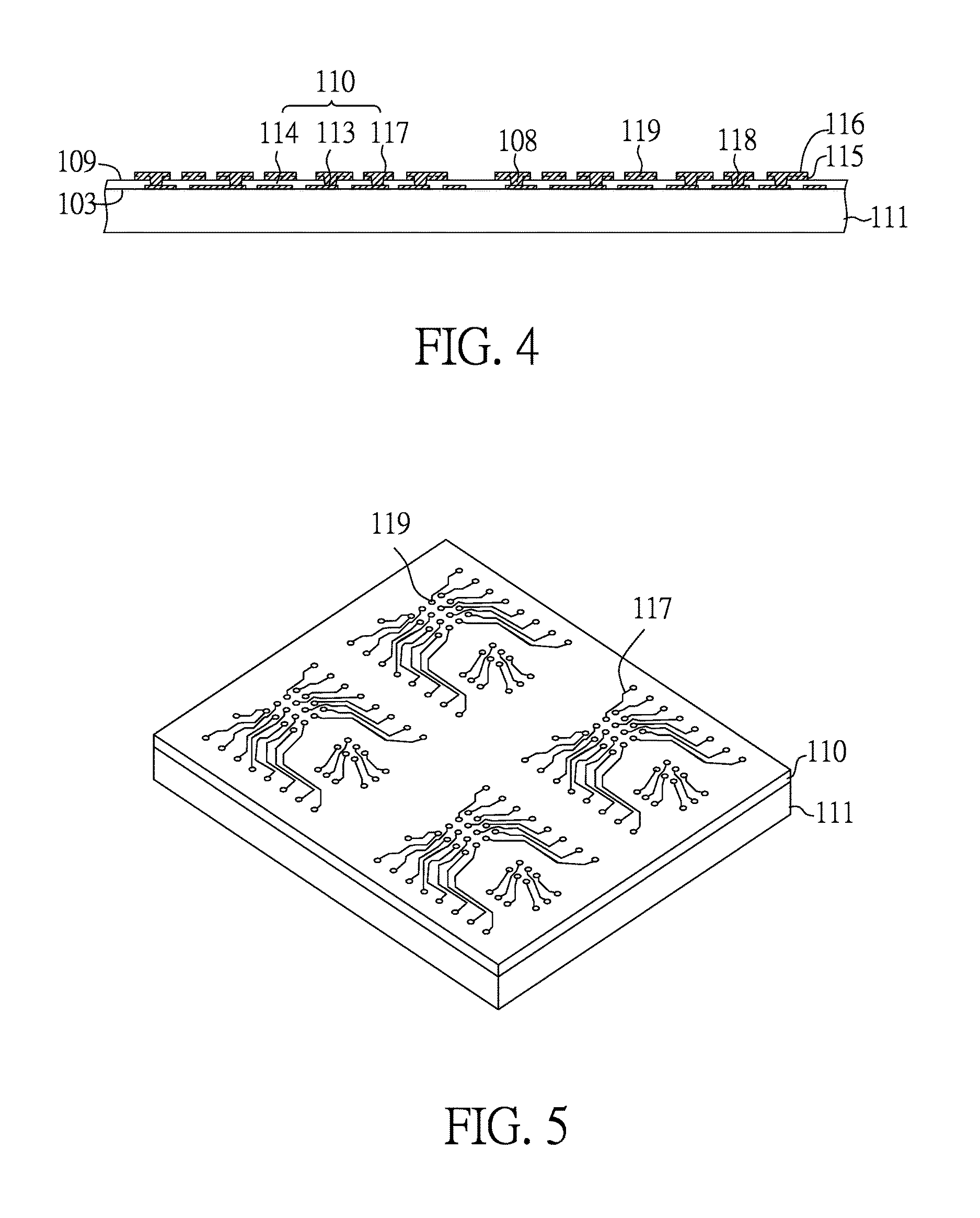
[0060]FIG. 1 is a cross-sectional view of the structure with first contact pads 113 deposited on a sacrificial carrier 111. The sacrificial carrier 111 typically can be made of any conductive or non-conductive material, such as copper, nickel, aluminum, chromium, tin, iron, stainless steel, silicon, glass, graphite, plastic film, or other metals, alloys or non-metallic materials. The thickness of the sacrificial carrier 111 preferably ranges from 0.1 to 10 mm. In this embodiment, the sacrificial carrier 111 is made of an iron-based material and has a thickness of 1.0 mm. The first contact pads 113 typically are made of copper and can be pattern deposited by numerous techniques, such as electroplating, electroless ...

embodiment 2

[0081]FIGS. 27-36 are cross-sectional views showing a method of making another semiconductor assembly in which the heat spreader has a registration mark outside its cavity and is further electrically coupled to the second build-up circuitry in accordance with another embodiment of the present invention.

[0082]For purposes of brevity, any description in Embodiment 1 above is incorporated herein insofar as the same is applicable, and the same description need not be repeated.

[0083]FIG. 27 is a cross-sectional view of a heat spreader 20 with a registration mark 213 around the entrance of cavities 211. The registration mark 213 can be formed by removing selected portions of a metal plate 21 or by pattern deposition of a metal or plastic material on the metal plate 21. Plating, etching, mechanical carving or lamination is typically used to form the registration mark 213. Accordingly, the registration mark 213 projects from the flat surface 212 of the heat spreader 20 adjacent to the cavit...

embodiment 3

[0093]FIGS. 37-46 are cross-sectional views showing a method of making yet another semiconductor assembly which uses a laminate substrate as the heat spreader in accordance with yet another embodiment of the present invention.

[0094]For purposes of brevity, any description in aforementioned Embodiments above is incorporated herein insofar as the same is applicable, and the same description need not be repeated.

[0095]FIGS. 37 and 38 are cross-sectional views showing a process of forming a registration mark on a dielectric layer of a laminate substrate in accordance with an embodiment of the present invention.

[0096]FIG. 37 is a cross-sectional view of a laminate substrate that includes a metal plate 21, a dielectric layer 23 and a metal layer 25. The dielectric layer 23 is sandwiched between the metal plate 21 and the metal layer 25. The dielectric layer 23 typically is made of epoxy resin, glass-epoxy, polyimide, or the like, and has a thickness of 50 microns. The metal layer 25 typic...


PUM


Abstract

The present invention relates to methods of making a semiconductor assembly having a semiconductor device embedded in a heat spreader and electrically connected to a dual-stage formed interconnect substrate. In a preferred embodiment, the interconnect substrate consists of first and second build-up circuitries and the methods are characterized by the step of attaching a semiconductor subassembly having a first build-up circuitry adhered to a sacrificial carrier to a heat spreader using an adhesive with the semiconductor device inserted into a cavity of the heat spreader and the step of detaching the sacrificial carrier from the first build-up circuitry. The heat spreader provides thermal dissipation, and the first and second build-up circuitries provide staged fan-out routing for the semiconductor device.

Description

FIELD OF THE INVENTION[0001]The present invention relates to a thermally enhanced semiconductor assembly, more particularly, to a thermally enhanced semiconductor assembly having a semiconductor device embedded in a heat spreader and electrically connected to dual-stage formed build-up circuitries and a method of making the same.DESCRIPTION OF RELATED ART[0002]The convergence of mobility, communication, and computing has created significant thermal, electrical, form-factor and reliability challenges to the semiconductor packaging industry. Despite numerous configurations for embedding semiconductor chip in wiring board or mold compound reported in the literature, many performance-related deficiencies remain. For example, the assemblies disclosed by U.S. Pat. Nos. 8,742,589, 8,735,222, 8,679,963, 8,453,323 may render performance degradation problems as the heat generated by the embedded chip can't be dissipated properly through the thermally insulating material such as laminate or mo...

Claims


Application Information

Patent Timeline
Patent Type & Authority Patents(United States)
IPC IPC(8): H01L23/367H01L23/544H01L21/78H01L21/48H01L23/498
CPCH01L23/3672H01L23/49811H01L23/49827H01L23/49822H01L21/4853H01L21/486H01L21/4857H01L21/4882H01L21/78H01L23/544H01L2223/54426H01L23/3675H01L23/49816H01L2224/73253H01L23/5383
Inventor LIN, CHARLES W. C.WANG, CHIA-CHUNG
Owner BRIDGE SEMICON
Learn More