
Optical electrical field enhancing device and measuring apparatus equipped with the device

a technology of optical electrical field and measuring apparatus, which is applied in the direction of optical radiation measurement, instruments, spectrometry/spectrophotometry/monochromators, etc., can solve the problems of difficult to receive weak raman light at a high s/n ratio, the sample itself becomes an obstruction to raman scattered light, etc., and achieves high degree of freedom in measurement , high sensitivity, the effect of high sensitivity

Inactive Publication Date: 2014-01-16
FUJIFILM CORP
View PDF6 Cites 10 Cited by
  • Summary
  • Abstract
  • Description
  • Claims
  • Application Information

AI Technical Summary

Benefits of technology

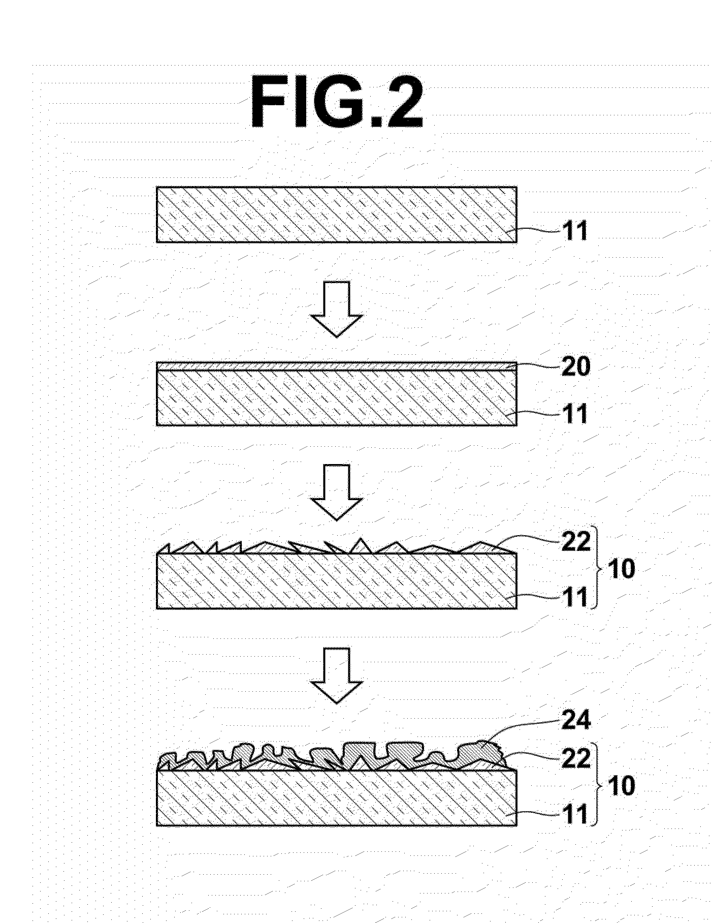
This patent describes a device that enhances the optical and electrical fields on the surface of a metal structure by using a process called plasmon resonance. This process involves shining light onto the metal structure and creating small metal particles that magnify the optical and electrical fields. The device can be made using a simple and inexpensive method of depositing metal onto a substrate and reacting it with water at high temperature. The technical effect of this invention is the creation of a device with enhanced optical and electrical fields, which can be utilized in various applications such as optical sensing and electronics.

Problems solved by technology

However, in the case that cells, which are samples having sizes on the order of micrometers, are test subjects, the sample itself becomes an obstruction to Raman scattered light.
Therefore, it had been difficult to receive weak Raman light at a high S / N ratio.

Method used


Image

  • Optical electrical field enhancing device and measuring apparatus equipped with the device
  • Optical electrical field enhancing device and measuring apparatus equipped with the device
  • Optical electrical field enhancing device and measuring apparatus equipped with the device

Examples


first embodiment

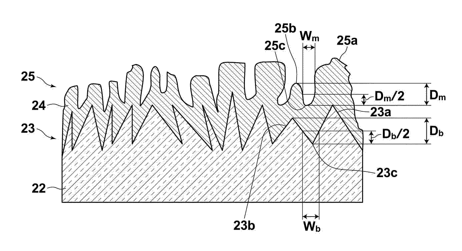
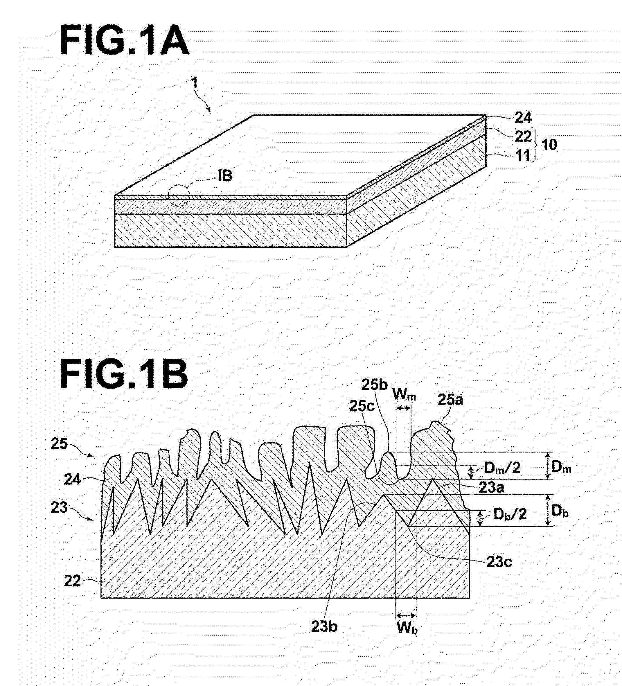
[0063]FIG. 1A is a perspective view that illustrates an optical electrical field enhancing substrate 1, which is a first embodiment of an optical electrical field enhancing device. FIG. 1B is a magnified view of a portion IB of the side surface of the optical electrical field enhancing substrate 1 illustrated in FIG. 1A.

[0064]As illustrated in FIG. 1A and FIG. 1B, the optical electrical field enhancing substrate 1 is constituted by a transparent substrate 10 having a structure of fine protrusions and recesses 23 on the surface thereof, and a metal structure layer of fine protrusions and recesses 24 formed on the surface of the structure of fine protrusions and recesses 23. Localized plasmon resonance is induced by light (hereinafter, excitation light) irradiated onto a structure of fine protrusions and recesses 25 of the metal structure layer of fine protrusions and recesses 24, and an enhanced optical electrical field is generated on the surface of the metal structure layer of fine...

second embodiment

[0089]An optical electrical field enhancing substrate 2, which is a second embodiment of the optical electrical field enhancing device of the present invention, will be described. FIG. 4A is a perspective view that illustrates the optical electrical field enhancing substrate 2 of the present embodiment. FIG. 4B is a magnified view of a portion IVB of a lower portion of the side surface of the optical electrical field enhancing substrate 2 illustrated in FIG. 4A.

[0090]The optical electrical field enhancing substrate 2 of the present embodiment is the optical electrical field enhancing substrate 1 of the first embodiment further equipped with a second transparent structure layer of fine protrusions and recesses 28 on the back surface thereof.

[0091]The second transparent structure layer of fine protrusions and recesses 28 is similar to the first transparent structure layer of fine protrusions and recesses 22 provided on the front surface of the transparent substrate 10, and may be cons...

third embodiment

[0094]A sample cell 3, which is a third embodiment of the optical electrical field enhancing device of the present invention, will be described. FIG. 6A is a plan view that illustrates an optical electrical field enhancing sample cell 3 as a third embodiment of the optical electrical field enhancing device. FIG. 6B is a sectional diagram of the optical electrical field enhancing sample cell 3 taken along line VIB-VIB of FIG. 6A.

[0095]The optical electrical field enhancing sample cell 3 of the present embodiment is equipped with: an optical electrical field enhancing substrate 30 constituted by a transparent substrate main body 31, a transparent structure layer of fine protrusions and recesses 32 provided on the surface of the transparent substrate main body 31, and a metal structure layer of fine protrusions and recesses 34 provided on the structure of fine protrusions and recesses 32; and a liquid sample holding member 35 provided on the metal structure layer of fine protrusions an...


PUM


Abstract

An optical electrical field enhancing device includes: a transparent substrate having a structure of fine protrusions and recesses on the surface thereof; and a metal structure layer of fine protrusions and recesses formed on the surface of the structure of fine protrusions and recesses. The metal structure layer of fine protrusions and recesses has a structure of fine protrusions and recesses, in which the distances among adjacent protrusions are less than the distances among corresponding adjacent protrusions of the structure of fine protrusions and recesses of the transparent substrate.

Description

TECHNICAL FIELD[0001]The present invention is related to an optical electrical field enhancing device equipped with a metal structure of fine protrusions and recesses capable of inducing localized plasmon, and a measuring apparatus equipped with the optical electrical field enhancing device.BACKGROUND ART[0002]Sensor devices that utilize the electrical field enhancing effect due to localized plasmon on the surfaces of metals and electrical field enhancing devices of Raman spectroscopic devices are known. Raman spectroscopy is a technique that obtains the spectrum of Raman scattered light (Raman spectrum) by spectrally analyzing scattered light obtained by irradiating a substance with a single wavelength light beam, and is utilized to identify substances.[0003]There is a Raman spectroscopy technique called SERS (Surface Enhanced Raman Scattering) that utilizes an optical electrical field enhanced by localized plasmon resonance in order to amplify weak Raman scattered light (refer to ...

Claims


Application Information

Patent Timeline
IPC IPC(8): G01N21/65H01S3/30
CPCG01N21/658H01S3/30B82Y20/00G01N21/554G01N21/648
Inventor YAMAZOE, SHOGONAYA, MASAYUKIHAKUTA, SHINYA
Owner FUJIFILM CORP
Learn More