
Electronic component

a technology of electronic components and components, applied in the field of electronic components, can solve the problems of difficult to achieve the land pattern change based on the land pattern, the vibration of the circuit board, and the mechanical distortion of the multilayer ceramic capacitor in some cases, so as to reduce the adhesion of the bonding agent, reduce the occurrence of vibration sound, and simple structure

Active Publication Date: 2014-01-16
MURATA MFG CO LTD
View PDF2 Cites 69 Cited by
  • Summary
  • Abstract
  • Description
  • Claims
  • Application Information

AI Technical Summary

Benefits of technology

The present invention provides an electronic component that is easy to design and mount, with strong mounting strength and good electrical characteristics. Additionally, it reduces or prevents vibration sounds.

Problems solved by technology

However, a multilayer ceramic capacitor is subject to mechanical distortion in some cases due to variations in the voltage applied to the multilayer ceramic capacitor.
When this distortion occurs, the distortion is transmitted to the circuit board, causing the circuit board to vibrate.
However, such an improvement based on changes to the land pattern is difficult to achieve for circuit boards currently in use which typically require high-density mounting.
Moreover, miniaturization is not easy to achieve, with the possibility of further increasing cost.
According to the configuration described in Japanese Unexamined Patent Application Publication No. 2010-123614, the multilayer ceramic capacitor is supported in midair by the conductive support member, which makes it difficult to achieve a reduction in height.
In addition, it is difficult to mount the multilayer ceramic capacitor with an appropriate spacing between the multilayer ceramic capacitor and the circuit board.
Further, because a flat-shaped conductor is used for the conductive support member, it is difficult to ensure sufficient mounting strength.

Method used


Image

  • Electronic component
  • Electronic component
  • Electronic component

Examples


Embodiment Construction

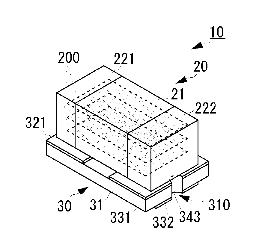
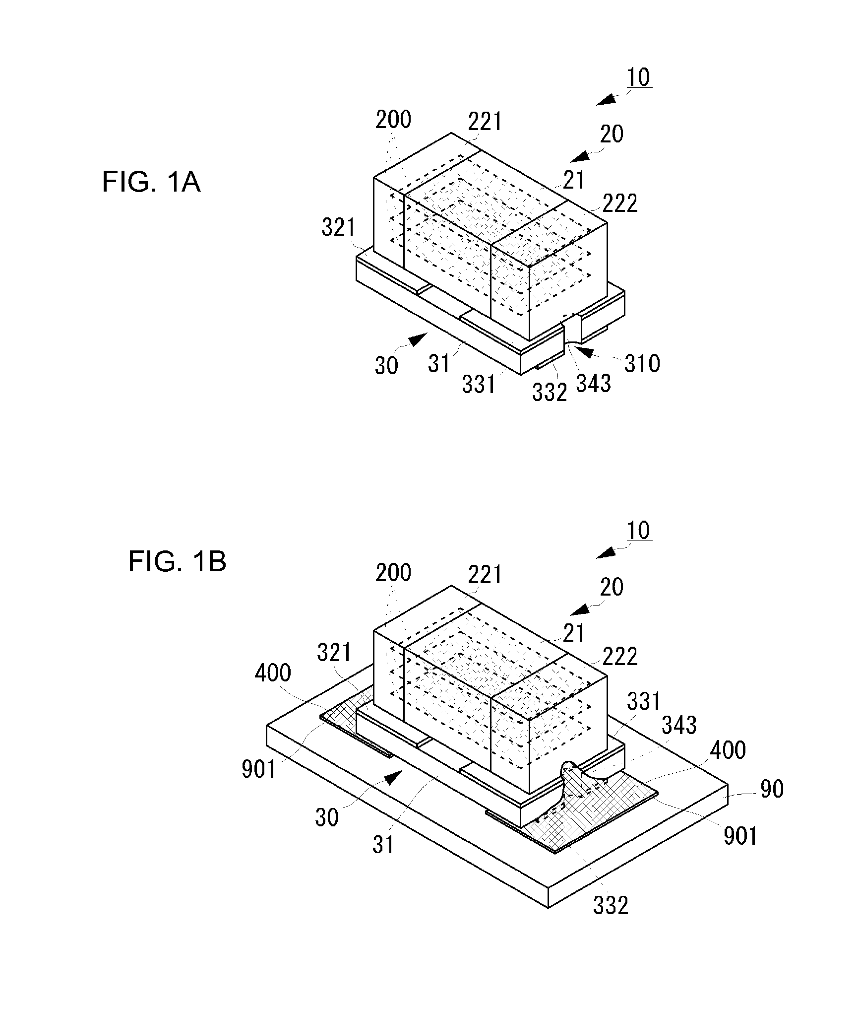
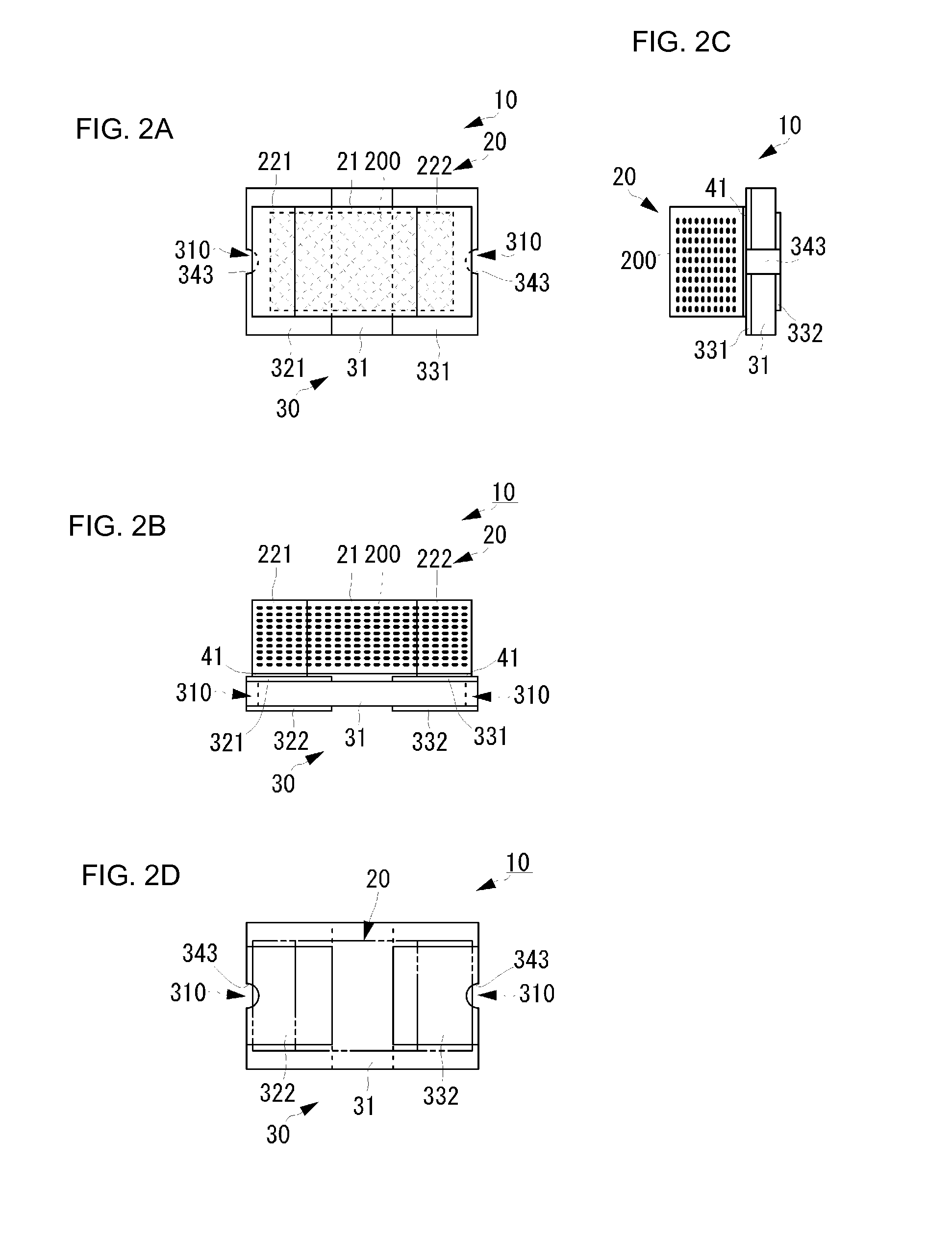
[0033]An electronic component according to a first preferred embodiment of the present invention will be described with reference to the drawings. FIG. 1A is a perspective view of the outward appearance of an electronic component 10 according to the first preferred embodiment. FIG. 1B is a perspective view of the mounting state of the electronic component 10. FIGS. 2A-2D are four-side views of the electronic component 10 according to the first preferred embodiment, of which FIG. 2A is a plan view, FIG. 2) is a first (longitudinal) side view, FIG. 2C is a second (lateral) side view, and FIG. 2D is a rear view. FIGS. 3A and 3B are a first side view and a second side view each illustrating the mounting state of the electronic component 10 according to the first preferred embodiment.

[0034]The electronic component 10 includes a multilayer ceramic capacitor 20 and an interposer 30. The interposer 30 corresponds to the “substrate” according to a preferred embodiment of the present inventio...


PUM

PropertyMeasurementUnit
Thicknessaaaaaaaaaa
Shapeaaaaaaaaaa
Areaaaaaaaaaaa

Abstract

A multilayer ceramic capacitor includes flat-shaped inner electrodes that are laminated. An interposer includes an insulating substrate that is larger than contours of the multilayer ceramic capacitor. A first mounting electrode that mounts the multilayer ceramic capacitor is located on a first principal surface of the insulating substrate, and a first external connection electrode for connection to an external circuit board located on a second principal surface. The multilayer ceramic capacitor is mounted onto the interposer in such a way that the principal surfaces of the inner electrodes are parallel or substantially parallel to the principal surface of the interposer, that is, the first and second principal surfaces of the insulating substrate.

Description

BACKGROUND OF THE INVENTION[0001]1. Field of the Invention[0002]The present invention relates to an electronic component including a multilayer ceramic capacitor, and an interposer that mounts the multilayer ceramic capacitor onto a circuit board.[0003]2. Description of the Related Art[0004]Currently, chip components, in particular, miniature multilayer ceramic capacitors are frequently used for mobile terminals such as cellular phones. A multilayer ceramic capacitor includes a rectangular component body that functions as a capacitor, and outer electrodes formed at opposite ends of the component body.[0005]In the related art, generally, as disclosed in Japanese Unexamined Patent Application Publication No. 8-55752, a multilayer ceramic capacitor is electrically and physically connected to a circuit board by placing outer electrodes directly on the mounting land of the circuit board of a mobile terminal, and bonding the mounting land and the outer electrodes together with a bonding a...

Claims


Application Information

Patent Timeline
IPC IPC(8): H01G4/01
CPCH01G4/01H01G2/06H05K1/0271H05K1/141H05K1/181H05K3/3442H05K2201/041H05K2201/049H05K2201/09181H05K2201/10015H05K2201/2045Y02P70/50H05K1/18H01G4/12H01G4/224H01G4/30
Inventor HATTORI, KAZUOFUJIMOTO, ISAMU
Owner MURATA MFG CO LTD
Learn More