
Layout-aware test pattern generation and fault detection

Active Publication Date: 2014-01-30
SYNOPSYS INC
View PDF2 Cites 6 Cited by
  • Summary
  • Abstract
  • Description
  • Claims
  • Application Information

AI Technical Summary

Benefits of technology

The patent describes techniques and systems for generating test patterns to detect faults in integrated circuits. The system receives a layout for the IC and generates a set of faults based on the layout. It then determines the likelihood of occurrence for each fault and generates a set of test patterns to target the faults based on their likelihood of occurrence. The system assigns weights to the faults based on their area of the layout and ranks the weights. It generates the test patterns based on a combination of random and deterministic patterns. The system also identifies a net in the layout and assigns a fault to each subnet in the net. The system uses an automatic test pattern generation engine and identifies subnets based on their routing area. Overall, the patent provides methods for efficiently detecting and targeting faults in ICs.

Problems solved by technology

This dramatic increase in semiconductor integration densities has made it considerably more challenging to efficiently test semiconductor devices after device manufacturing.
Defects (systematic and random) introduced during manufacturing process may cause a signal line to get broken or shorted with another line resulting in the manufactured chip to fail.
Moreover, a semiconductor chip may meet timing constraints during the design phase, however, a manufactured semiconductor chip may contain defects, due to process variations and other factors, which may result in a delay violation causing the chip to fail.
Usually, a pattern generated to detect a single fault ends up fortuitously detecting many other faults.
Note that it is impractical to cover all possible faults on millions of sites within a reasonable amount of time.
As a result, faults that are harder to test are not sufficiently covered by the conventional techniques.
However, as acceptable DPPM levels continue to decrease and IC manufacturers aggressively pursue an objective of near zero DPPM, the conventional ATPG techniques have become increasingly ineffective.
Another potential problem associated with conventional ATPG techniques lies in the fact that high fault coverage usually does not guarantee high defect coverage.
As a result, the high risk faults are often not treated effectively with the current techniques.
For example, when an ATPG technique achieves 98% fault coverage, the remaining 2% of the uncovered faults can represent significantly more than 2% of the risk of defects.

Method used


Image

  • Layout-aware test pattern generation and fault detection
  • Layout-aware test pattern generation and fault detection
  • Layout-aware test pattern generation and fault detection

Examples


Embodiment Construction

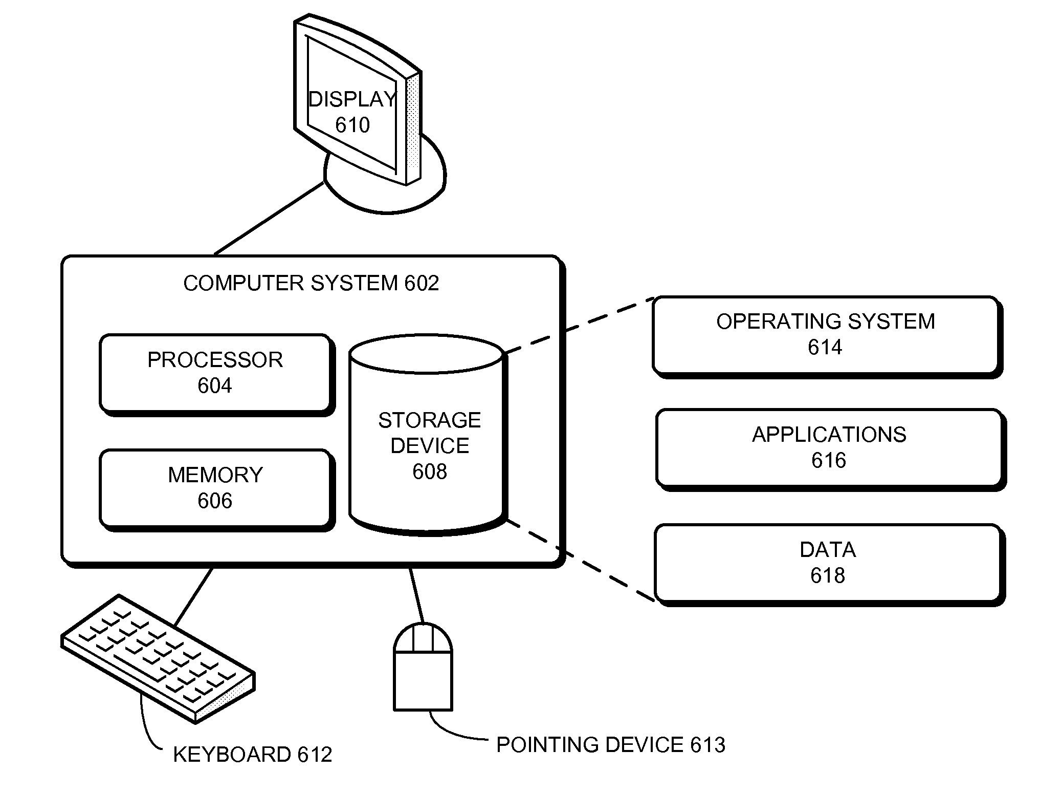
[0030]The following description is presented to enable any person skilled in the art to make and use the embodiments, and is provided in the context of a particular application and its requirements. Various modifications to the disclosed embodiments will be readily apparent to those skilled in the art, and the general principles defined herein may be applied to other embodiments and applications without departing from the spirit and scope of the present disclosure. Thus, the present invention is not limited to the embodiments shown, but is to be accorded the widest scope consistent with the principles and features disclosed herein.

[0031]The data structures and code described in this disclosure can be partially or fully stored on a non-transitory computer-readable storage medium and / or a hardware module and / or hardware apparatus. A non-transitory computer-readable storage medium includes all computer-readable storage mediums with the sole exception of a propagating electromagnetic wa...


PUM


Abstract

Methods and apparatuses to generate test patterns for detecting faults in an integrated circuit (IC) are described. During operation, the system receives a netlist and a layout for the IC. The system then generates a set of faults associated with the netlist to model a set of defects associated with the IC. Next, the system determines a set of likelihoods of occurrence for the set of faults based at least on a portion of the layout associated with each fault in the set of faults. The system subsequently generates a set of test patterns to target the set of faults, wherein the set of test patterns are generated based at least on the set of likelihoods of occurrence associated with the set of faults.

Description

BACKGROUND[0001]1. Technical Field[0002]The present invention relates to techniques for testing semiconductor chips. More specifically, the present invention relates to methods and apparatuses for generating test patterns for detecting faults in semiconductor chips.[0003]2. Related Art[0004]Advances in semiconductor technology presently make it possible to integrate large-scale systems, including hundreds of millions of transistors, onto a single semiconductor chip. This dramatic increase in semiconductor integration densities has made it considerably more challenging to efficiently test semiconductor devices after device manufacturing. Defects (systematic and random) introduced during manufacturing process may cause a signal line to get broken or shorted with another line resulting in the manufactured chip to fail. Moreover, a semiconductor chip may meet timing constraints during the design phase, however, a manufactured semiconductor chip may contain defects, due to process variat...

Claims


Application Information

Patent Timeline
IPC IPC(8): G01R31/00G06F19/00
CPCG01R31/318371
Inventor SANYAL, ALODEEPPATANKAR, GIRISH A.KAPUR, ROHITTALLUTO, SALVATORE
Owner SYNOPSYS INC
Learn More