Semiconductor manufacturing device and manufacturing method thereof

a manufacturing device and semiconductor technology, applied in the direction of mechanical equipment, water supply installation, transportation and packaging, etc., can solve the problems of defective contacts, decrease in signal transmission speed of semiconductor devices, increase in power consumption, etc., to prevent the oxidation of metal layers, increase power consumption, and prevent the effect of occurren

Inactive Publication Date: 2014-02-06
WONIK IPS CO LTD
View PDF4 Cites 4 Cited by
  • Summary
  • Abstract
  • Description
  • Claims
  • Application Information

AI Technical Summary

Benefits of technology

The present invention relates to a method for preventing the oxidation of a metal layer on a semiconductor device during a process transfer. By using an oxidation preventing gas in the transfer chamber and / or loadlock chamber, the contact resistance of the metal layer is not increased, which prevents problems such as an increase in power consumption and a decrease in signal transmission speed.

Problems solved by technology

This may lead to defective contacts, resulting in, for example, cracks in the semiconductor device.
The oxidized copper leads to an increase in contact resistance, which results in a number of problems, such as an increase in power consumption and a decrease in signal transmission speed of the semiconductor device.

Method used


Image

  • Semiconductor manufacturing device and manufacturing method thereof
  • Semiconductor manufacturing device and manufacturing method thereof
  • Semiconductor manufacturing device and manufacturing method thereof

Examples


Embodiment Construction

[0005]Technical Objective

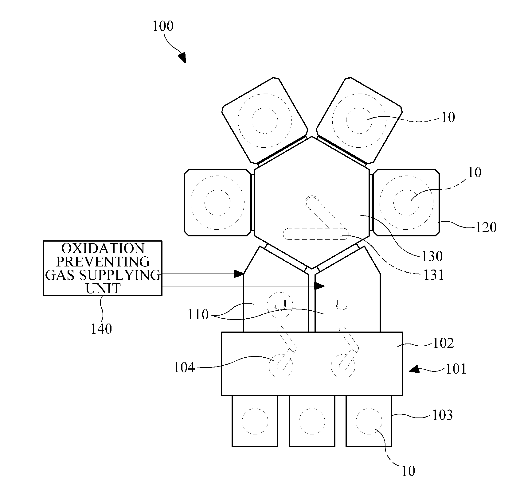
[0006]The technical objective of the present invention is to provide a semiconductor manufacturing device and manufacturing method capable of preventing the oxidation of a metal layer or the like of a substrate during an annealing process on the substrate.

[0007]Technical Solution

[0008]According to an exemplary embodiment of the present invention, a semiconductor manufacturing device may include: a loadlock chamber; one or more process chamber configured to receive a substrate and perform an annealing process; a transfer chamber configured to transfer the substrate between the loadlock chamber and the process chamber; and an oxidation preventing gas supplying unit configured to supply an oxidation preventing gas to at least one of the transfer chamber and the loadlock chamber.

[0009]According to another exemplary embodiment of the present invention, a semiconductor manufacturing method may include: transferring a substrate into a process chamber from a loadloc...


PUM


Abstract

The present invention relates to a semiconductor manufacturing device, which can be applied in a semiconductor metal interconnection process, and a manufacturing method thereof. The semiconductor manufacturing device includes a loadlock chamber, at least one process chamber, a transfer chamber, and an oxidation preventing gas supply unit. The process chamber processes an annealing process by receiving a substrate. The transfer chamber transfers the substrate between the loadlock chamber and the process chamber. The oxidation preventing gas supply unit supplies oxidation preventing gas into either the transfer chamber or the loadlock chamber.

Description

TECHNICAL FIELD[0001]The following description relates to a semiconductor manufacturing device and method, and more particularly, to a semiconductor manufacturing device and method applicable to a semiconductor metal wiring process.BACKGROUND ART[0002]Generally, aluminum, featuring in low cost and favorable properties, has been widely used for a semiconductor metal wiring process. Recently, however, the use of copper has been increasing to obtain a faster signal transmission speed of a semiconductor device. Copper has lower resistance properties and greater electromigration resistance than aluminum.[0003]A copper wiring process includes operations of: sequentially stacking a conductive layer and an insulating layer on a substrate, such as a wafer; and forming a contact hole passing through the insulating layer. Copper is inserted into the contact hole, and then the planarization is performed on the inserted copper surface by use of chemical mechanical polishing. Thereafter, the subs...

Claims


Application Information

Patent Timeline
Patent Type & Authority Applications(United States)
IPC IPC(8): F17D1/04
CPCF17D1/04H01L21/67196H01L21/67201H01L21/76883Y10T137/6966Y10T137/0318
Inventor LEE, KI-HOONRYU, DONG-HO
Owner WONIK IPS CO LTD
Why Eureka
Try Eureka