Planar electronic device

Inactive Publication Date: 2014-02-13
TE CONNECTIVITY CORP
View PDF7 Cites 46 Cited by
  • Summary
  • Abstract
  • Description
  • Claims
  • Application Information

AI Technical Summary

Benefits of technology

[0005]A need exists for planar electron

Problems solved by technology

The layout of such conductors may have adjacent primary and secondary sections that are different (e.g. one short and one long), which negatively affects the performance of the planar electronic device.
Additionally, some conduct

Method used


Image

  • Planar electronic device
  • Planar electronic device
  • Planar electronic device

Examples


Example

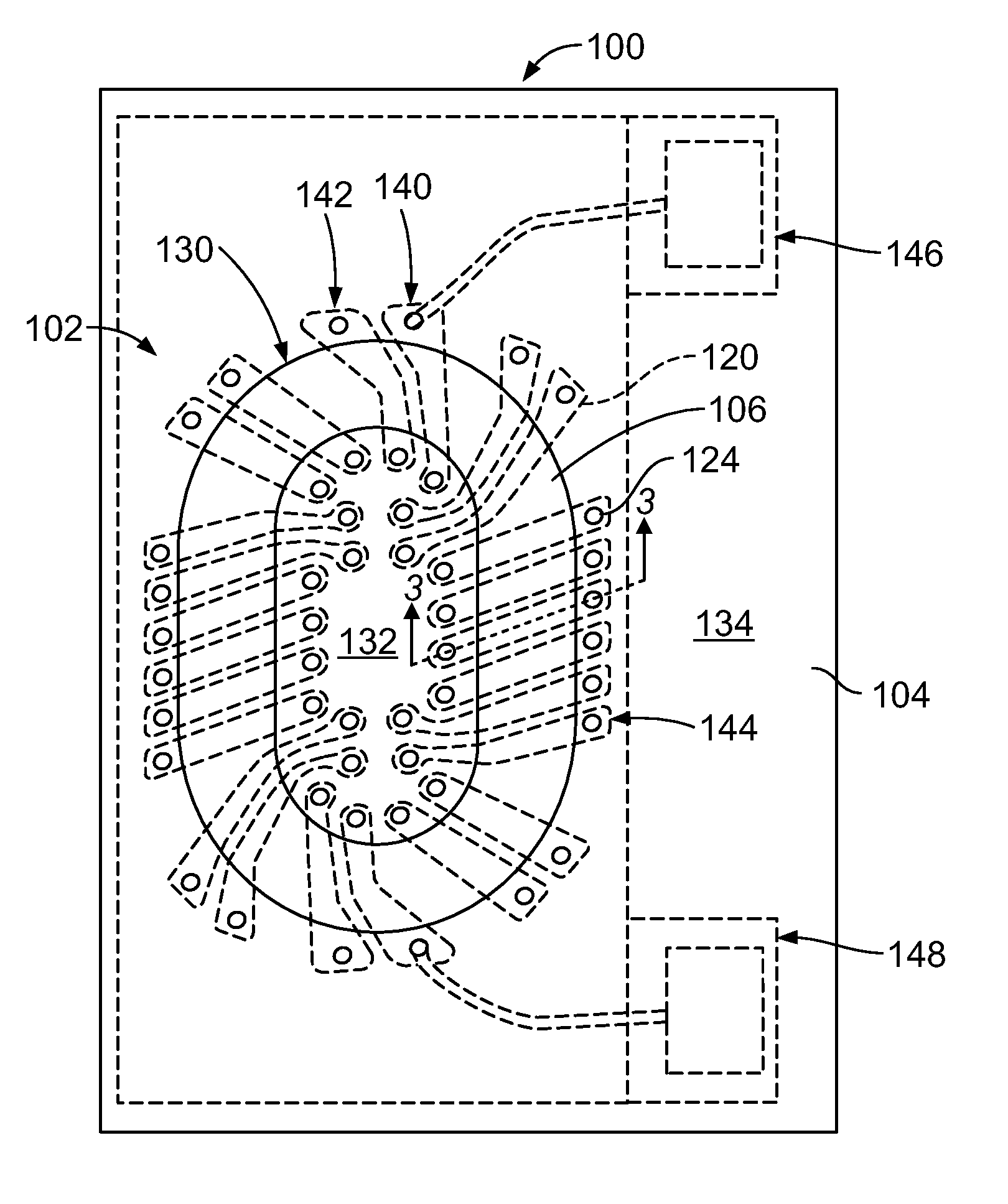
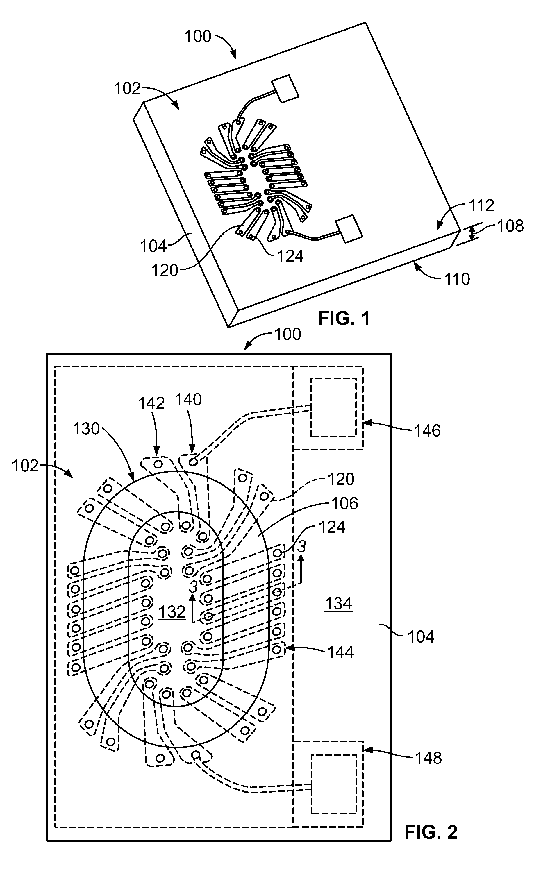
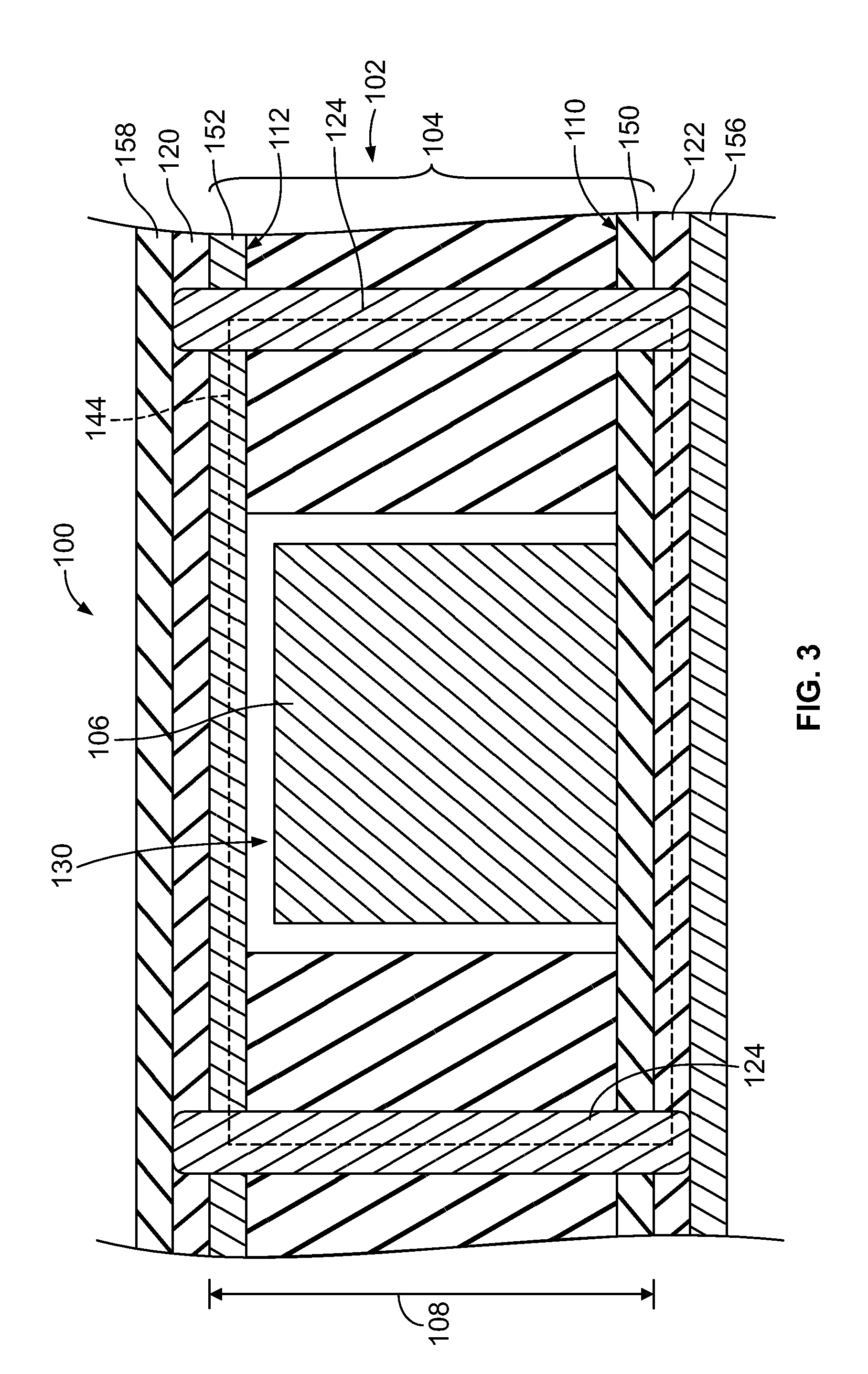
[0017]FIG. 1 is a perspective view of one embodiment of a planar electronic device 100 having a magnetic component 102. The magnetic component 102 shown in FIG. 1 is a transformer device. Alternatively, the magnetic component 102 may be or include another electronic device or component, such as an inductor, filter, balun, coupler, and the like, that includes a ferrite body or other magnetic material. The magnetic component 102 is disposed in a planar dielectric or non-conductive substrate 104. The substrate 104 holds a ferrite material body 106 (shown in FIG. 2). The illustrated magnetic component 102 has an oval shape, but alternatively may have a different shape, such as a circular shape.

[0018]The substrate 104 has a thickness dimension 108 that is measured between a lower side 110 and an opposite upper side 112 of the substrate 104. As used herein, the terms “lower” and “upper” or “top” and “bottom” are used to refer to the opposite sides of the substrate 104. The use of the term...


PUM


Abstract

A planar electronic device includes top conductors on a top side of a planar substrate connected to conductive vias and defining top conductor groups and bottom conductors on a bottom side connected to corresponding vias and defining bottom conductor groups. The conductors and vias define primary and secondary conductive loops with the top conductor group including at least one primary top conductor and at least one secondary top conductor and with the bottom conductor group including at least one primary bottom conductor and at least one secondary bottom conductor. The top conductors within each group have substantially similar layouts that are different from layouts of the immediately adjacent groups, and the bottom conductors within each group have substantially similar layouts that are different from layouts of the immediately adjacent groups.

Description

BACKGROUND OF THE INVENTION[0001]The subject matter herein relates generally to planar electronic devices, such as transformers, inductors, baluns, couplers, or filters.[0002]Some known electronic devices include planar bodies, such as circuit boards, that include one or more magnetic components built into the planar bodies. The magnetic component can include a ferrite core with conductive winding extending around the ferrite core. Some of these magnetic components include two conductive windings that are not conductively coupled with each other. For example, the conductive windings may not be physically or mechanically coupled such that electric current cannot flow through one conductive winding directly onto the other conductive winding. The current flowing through one winding generates a magnetic field in the core and in the other winding. The magnetic field in the other winding generates an electric current in the other winding. The electrical performance of the device can be de...

Claims


Application Information

Patent Timeline
IPC IPC(8): H01F5/00H03H7/01H03H7/42
CPCH01F17/0006H01F17/0033H01F27/2804
Inventor DALMIA, SIDHARTHMCGRATH, MARK PATRICKZHUOWEN, SUNNGUYEN, KHANH
Owner TE CONNECTIVITY CORP
Why Eureka
Try Eureka