

Semiconductor device and method of manufacturing the same
- Summary
- Abstract
- Description
- Claims
- Application Information
AI Technical Summary
Benefits of technology
Problems solved by technology
Method used
Image

Examples
first embodiment
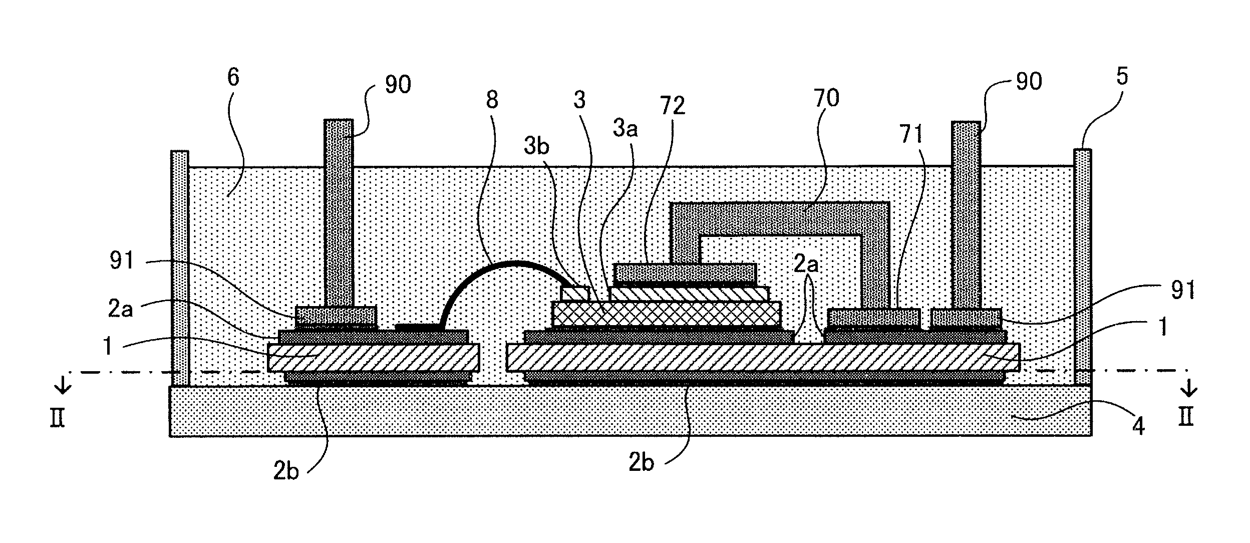
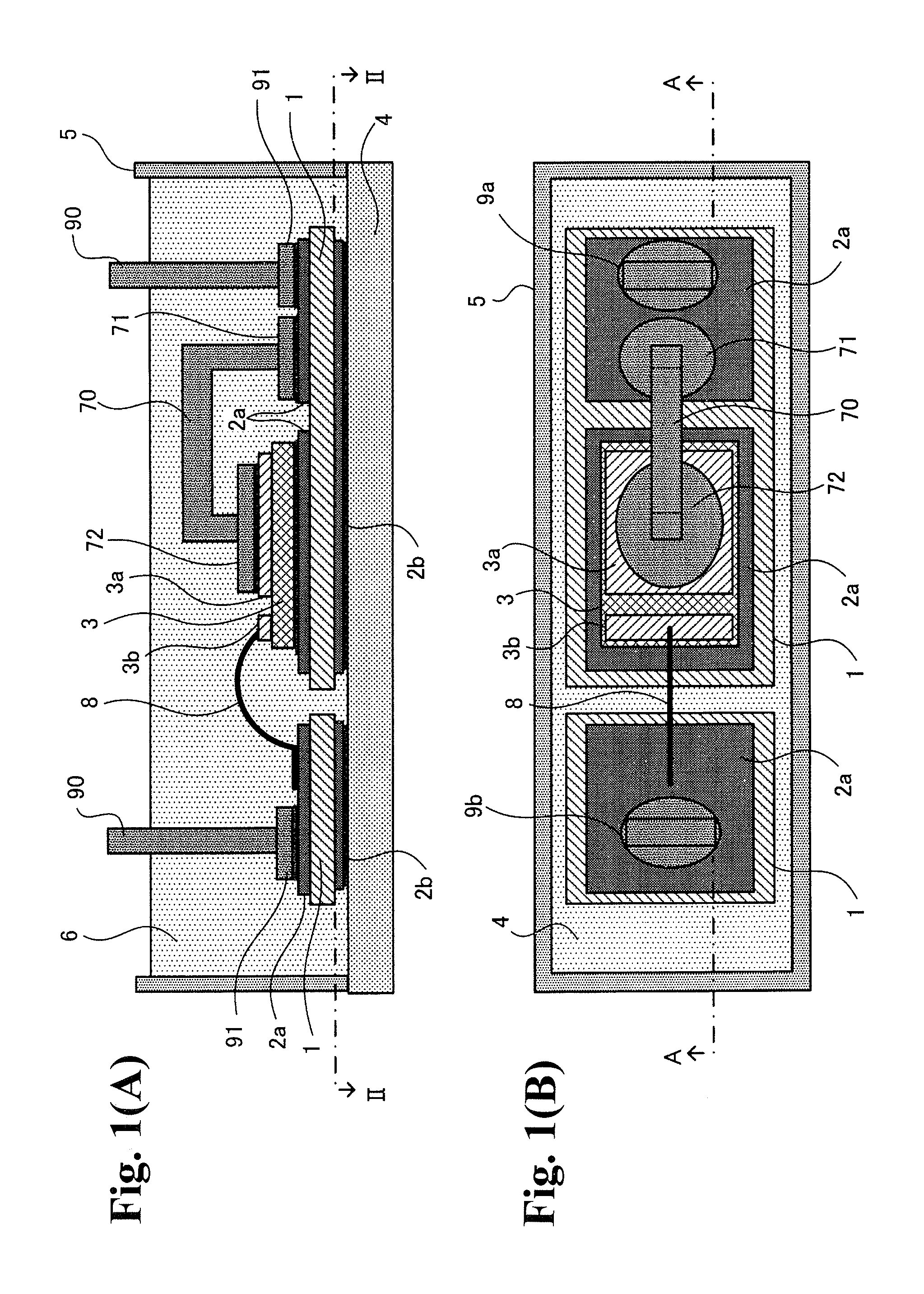
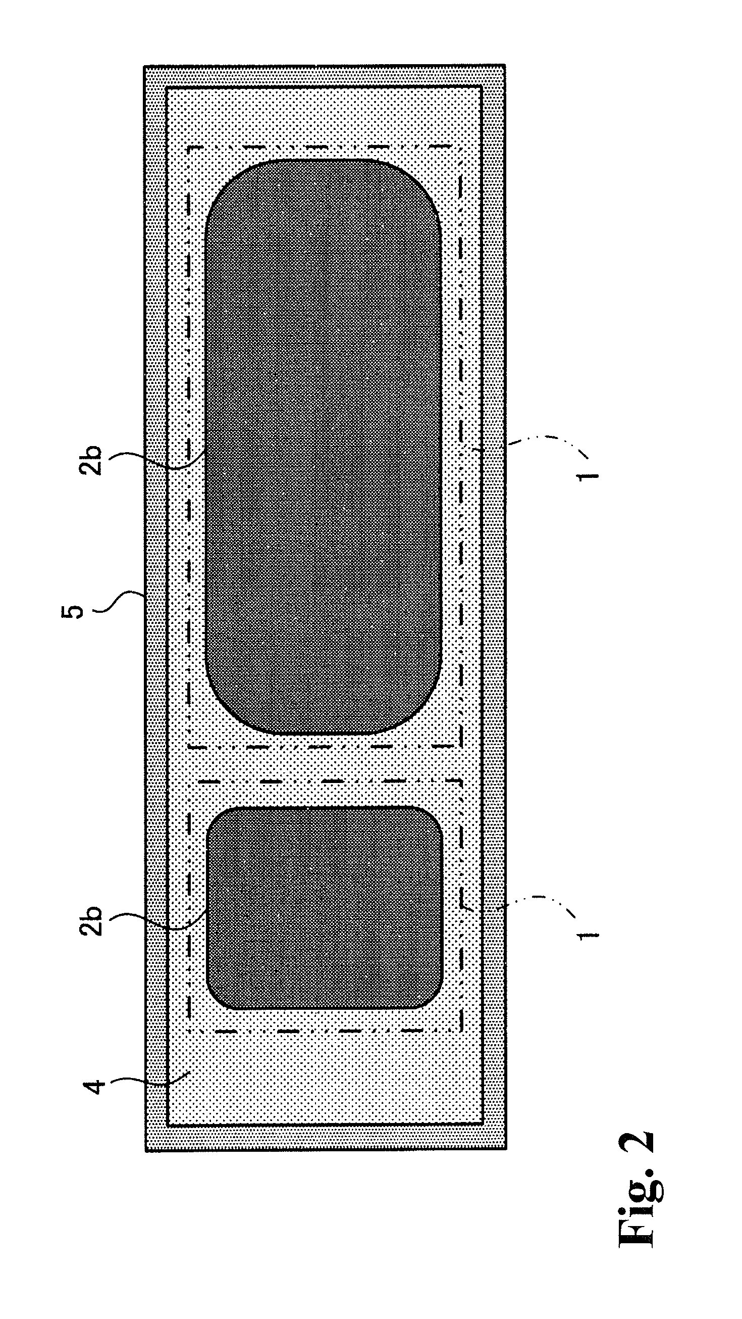
[0034]Hereinafter, embodiments of the invention will be described with reference to the accompanying drawings. FIGS. 1(A), 1(B) are a vertical cross-sectional view and a plan view illustrating a semiconductor device according to the invention. FIG. 2 is a cross-sectional view taken along the line II-II of FIG. 1(A).
[0035]In the power semiconductor device illustrated in the figure, a semiconductor chip 3 is mounted on an insulating substrate 1 having conductor patterns 2a and 2b bonded to the front and rear surfaces thereof, and the insulating substrate 1 is bonded to a heat-dissipating base member 4. In this way, it is possible to dissipate heat generated from the semiconductor chip 3 to the outside. In addition, in the power semiconductor device, external lead terminals 9a, 9b, which are lead frames of copper plates, are bonded to the conductor pattern 2a on the front surface of the insulating substrate 1 having the semiconductor chip 3 mounted thereon. The power semiconductor devi...
second embodiment
[0049]FIGS. 4(a), 4(B) are diagrams illustrating a bonding state between a heat-dissipating base member and an insulating substrate of a semiconductor device according to the invention.
[0050]Conductor patterns including four and ten divided conductor layers 2c are provided on the rear surfaces of insulating substrates 1a, 1b which are bonded to the heat-dissipating base member 4, respectively. Each of the conductor layers 2c has a rectangular pattern shape with rounded corners. In this way, it is possible to reduce the size of a solder fixing layer 13 for fixing each conductor layer 2c to the heat-dissipating base member 4.
[0051]That is, the length L of the second metal member 12 illustrated in FIG. 3 is reduced and the shear strain rate Δγ acting on the fixing layer 13 is reduced from the above-mentioned Expression 1. Therefore, the occurrence of a crack is prevented and it is possible to prevent the thermal fracture of the semiconductor device. The number of divided conductor laye...
third embodiment
[0052]FIGS. 5(A)-5(C) are diagrams illustrating a bonding state between a heat-dissipating base member and an insulating substrate of a semiconductor device according to the invention.
[0053]The power semiconductor device includes bonding portions 20 which protrude from a plurality of divided regions of a conductor pattern 2b on the rear surface of the insulating substrate bonded to a heat-dissipating base member 4 to the heat-dissipating base member 4. In this case, it is possible to reduce the size of a solder fixing layer 13 for fixing each of the bonding portions 20 to the heat-dissipating base member 4.
PUM
 Abstract
Description
Claims
Application Information