
Substrate for color conversion of light-emitting diode and manufacturing method therefor

Inactive Publication Date: 2017-08-24
SAMSUNG CORNING PRECISION MATERIALS CO LTD
View PDF16 Cites 2 Cited by
  • Summary
  • Abstract
  • Description
  • Claims
  • Application Information

AI Technical Summary

Benefits of technology

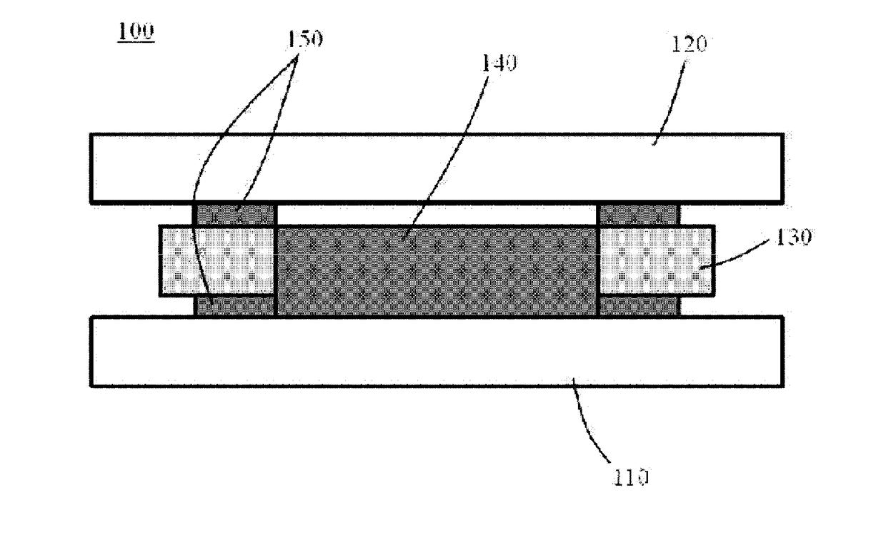
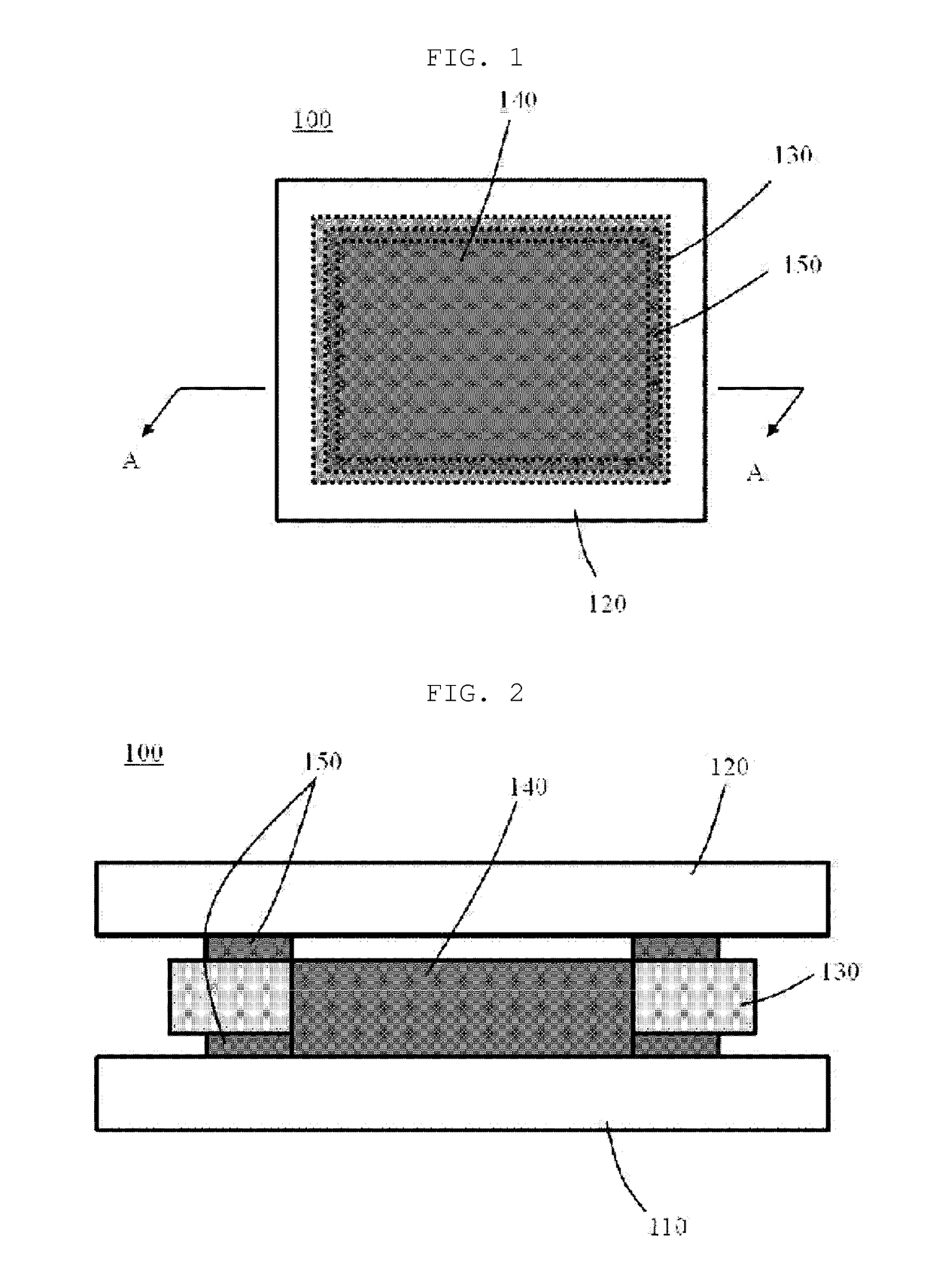
The present patent describes a new technology for improving the lifespan and efficiency of LED displays. The technology involves using a structural body containing a yellow fluorescent material and a low melting point glass frit to convert the blue light emitted by the LEDs into white light. This yellow fluorescent material also acts as a color conversion material, which increases the lifespan of the LED and display device. The structural body is bonded to the substrates using a low melting point glass frit sealant, providing excellent protection for the QDs. Overall, this technology improves the performance and reliability of LED displays.

Problems solved by technology

However, color tones may change depending on the environment in which such devices are used, since individual monochromatic LEDs have different thermal or temporal characteristics.
In particular, color stains may occur, making it difficult to uniformly mix different colors of light.
However, this related-art method is problematic in that fabrication costs are relatively high, due to the barrier layers needing to be applied several times, and most of all, this method fails to entirely protect the QDs from the external environment.
However, the etching process may cause fabrication costs to be increased.
In particular, it may be difficult to use a thin glass plate.
The use of QDs consequently leads to a problem in that it may be difficult to obtain or ensure the lifespan of an LCD using a QD-LED backlight.

Method used


Image

  • Substrate for color conversion of light-emitting diode and manufacturing method therefor
  • Substrate for color conversion of light-emitting diode and manufacturing method therefor
  • Substrate for color conversion of light-emitting diode and manufacturing method therefor

Examples


Embodiment Construction

[0040]Reference will now be made in detail to a color conversion substrate for a light-emitting diode (LED) and a method of fabricating the same according to the present disclosure, embodiments of which are illustrated in the accompanying drawings and described below, so that a person skilled in the art to which the present disclosure relates could easily put the present disclosure into practice.

[0041]Throughout this document, reference should be made to the drawings, in which the same reference numerals and symbols will be used throughout the different drawings to designate the same or like components. In the following description, detailed descriptions of known functions and components incorporated herein will be omitted in the case that the subject matter of the present disclosure is rendered unclear by the inclusion thereof.

[0042]As illustrated in FIG. 1 and FIG. 2, the LED color conversion substrate 100 according to the present embodiment is a substrate disposed over an LED, en...


PUM

PropertyMeasurementUnit
Melting pointaaaaaaaaaa
Fluorescenceaaaaaaaaaa

Abstract

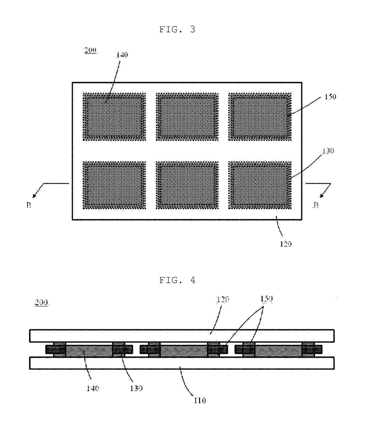
The present invention relates to a substrate for the color conversion of a light-emitting diode and a manufacturing method therefor and, more specifically, to a substrate for the color conversion of a light-emitting diode and a manufacturing method therefor, which enable a quantum dot (QD) and a structure, in which the QD is supported, to have a color conversion function for implementing white light. To this end, the present invention provides a substrate for the color conversion of a light-emitting diode, comprising: a first glass substrate arranged on a light-emitting diode; a second glass substrate formed to face the first glass substrate; a structure arranged between the first glass substrate and the second glass substrate, having a hollow portion and formed from a mixture of a yellow phosphor and a low-melting point frit glass; a QD filling the hollow portion; and sealing materials respectively formed between the first glass substrate and the lower side of the structure and between the second glass substrate and the upper side of the structure.

Description

BACKGROUND[0001]Field[0002]The present disclosure generally relates to a color conversion substrate for a light-emitting diode (LED) and a method of fabricating the same. More particularly, the present disclosure relates to a color conversion substrate for an LED, in which not only a quantum dot (QD) but also a structural body containing the QD has a color conversion function for producing white light, and a method of fabricating the same.[0003]Description of Related Art[0004]A light-emitting diode (LED) is a semiconductor device formed of a compound such as gallium arsenide (GaAs) to emit light when an electrical current is applied thereto. The LED uses a p-n junction semiconductor structure into which minority carriers, such as electrons or holes, are injected, such that light is generated by the recombination of electrons and holes.[0005]The characteristics of LEDs include low power consumption, a relatively long lifespan, the ability to be mounted in cramped spaces, and strong r...

Claims


Application Information

Patent Timeline
IPC IPC(8): H01L33/50C09K11/77C03C8/04C03C8/14C03C4/12C03C8/08H01L33/56C09K11/02
CPCH01L33/505H01L33/502H01L33/56C09K11/7706C09K11/025C03C8/14C03C2207/00C03C8/08C03C8/04H01L2933/0083H01L2933/0041H01L2933/005C03C2204/00C03C4/12H01L33/501Y02B20/00H01L33/50H01L33/52
Inventor LEE, KI YEONOH, YOON SEUKMOON, HYUNG SOO
Owner SAMSUNG CORNING PRECISION MATERIALS CO LTD
Learn More