Electroconductive sheet and touch panel

a technology of conductive sheets and touch panels, applied in the direction of circuit optical details, programmable/customizable/modifiable circuits, instruments, etc., can solve the problems of deteriorating the detection sensitivity of touch positions, the touch panel electrode of thin metal wires has problems with transparency and visibility, etc., and achieves high transparency. , the effect of high transparency

Inactive Publication Date: 2014-02-27
FUJIFILM CORP
View PDF7 Cites 61 Cited by
  • Summary
  • Abstract
  • Description
  • Claims
  • Application Information

AI Technical Summary

Benefits of technology

[0009]In general, the visibility can be improved by reducing the line width of the thin metal wires. However, the electrode containing the thin metal wires with the reduced line width disadvantageously has an increased resistance, which deteriorates the touch position detection sensitivity. Therefore, it is necessary to optimize the shapes of the conductive pattern and the thin metal wire pattern.
[0038]As described above, the conductive sheet and the touch panel of the present invention can have the electrodes containing the patterns of less-visible, thin, metal wires and can exhibit a high transparency.

Problems solved by technology

The touch panel electrode of the thin metal wires has problems with transparency and visibility because the thin metal wires are composed of an opaque material.
However, the electrode containing the thin metal wires with the reduced line width disadvantageously has an increased resistance, which deteriorates the touch position detection sensitivity.

Method used


Image

  • Electroconductive sheet and touch panel
  • Electroconductive sheet and touch panel
  • Electroconductive sheet and touch panel

Examples


examples

[0215]The present invention will be described more specifically below with reference to Examples. Materials, amounts, ratios, treatment contents, treatment procedures, and the like, used in Examples, may be appropriately changed without departing from the scope of the present invention. The following specific examples are therefore to be considered in all respects as illustrative and not restrictive.

first example

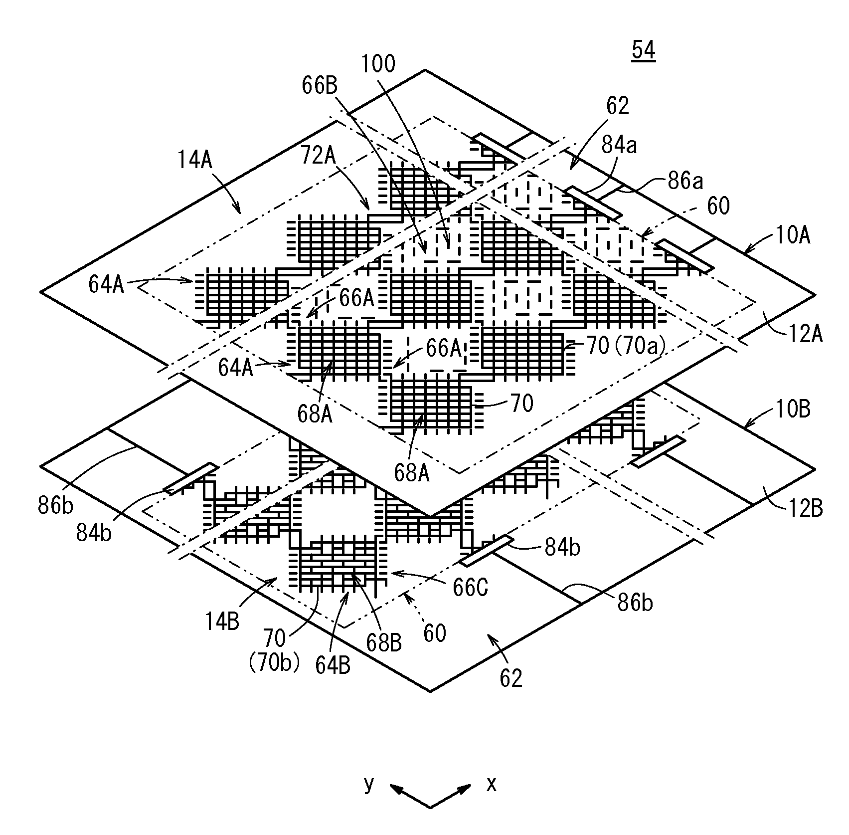
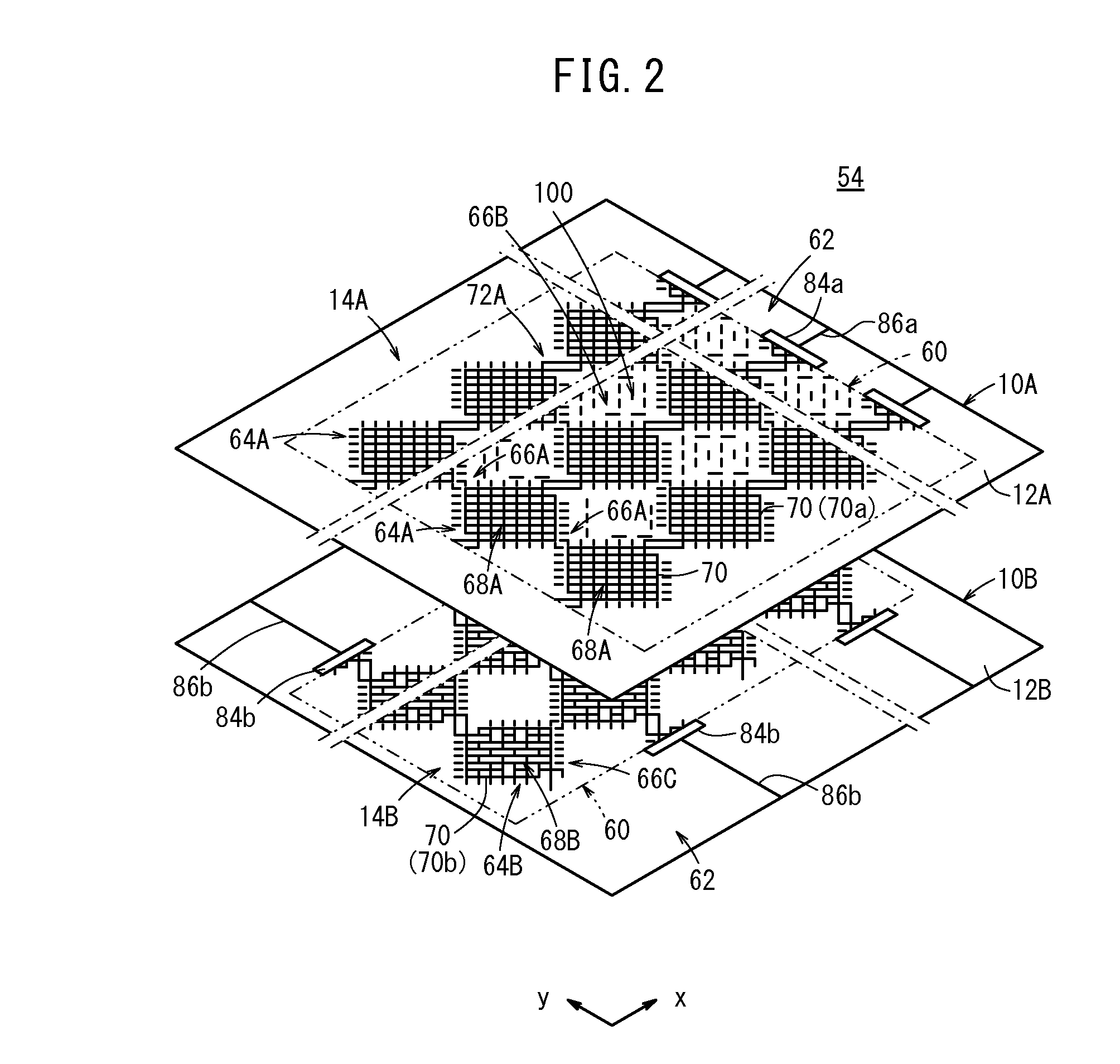
[0216]In First Example, in Examples 1 to 4 and Comparative Example 1, the visibility of the conductive sheet stack 54 was evaluated. The properties, measurement results, and evaluation results of Examples 1 to 4 and Comparative Example 1 are shown in Table 3.

second example

[0230]In Second Example, the visibilities of Samples 1 to 49 were evaluated. With respect to the visibility, the visual finding difficulty of the thin metal wires and transmittance were evaluated. The properties and evaluation results of Samples 1 to 49 are shown in Tables 4 and 5.

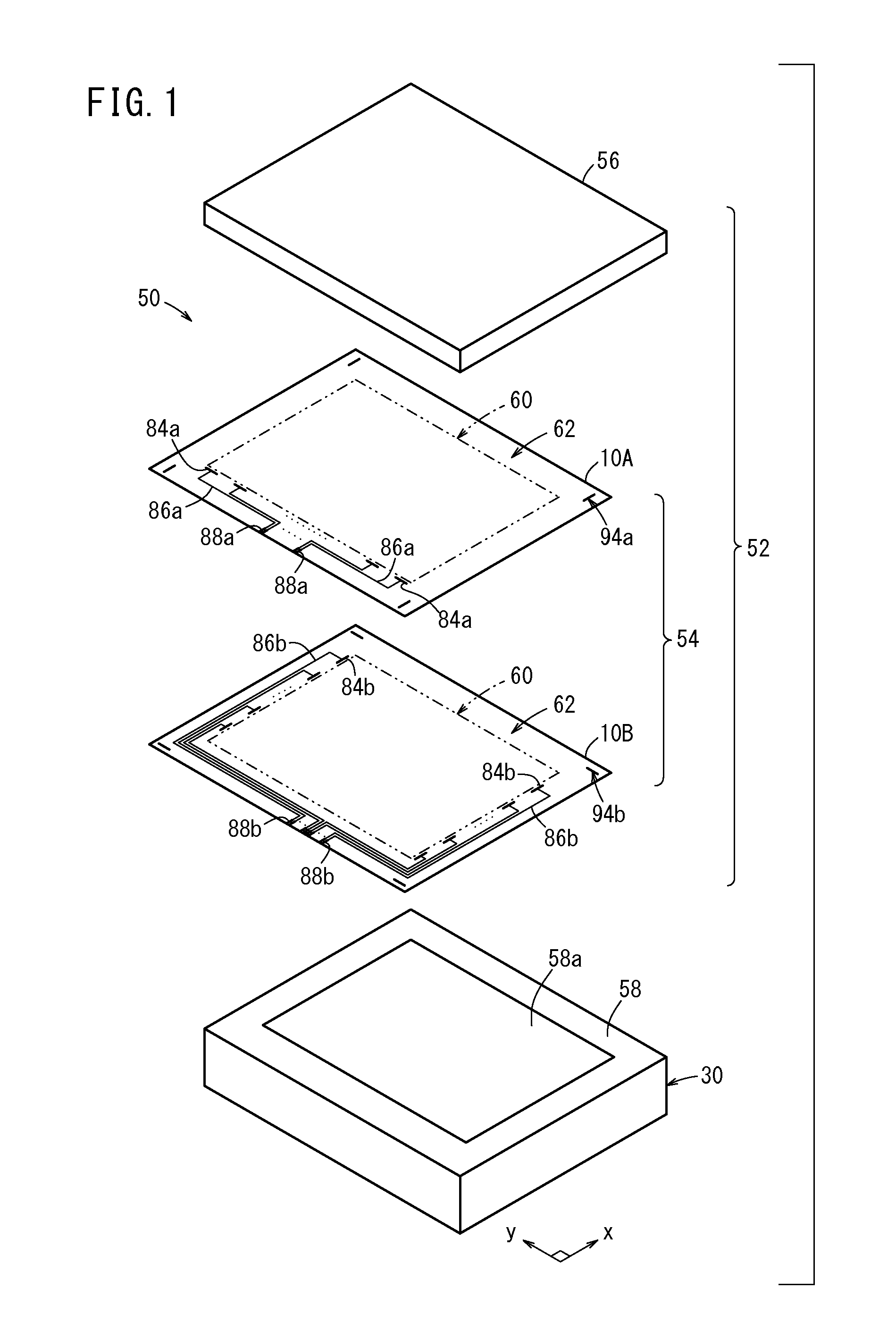
[0231]The photosensitive silver halide material was prepared in the same manner as Example 1 in First Example, and the photosensitive silver halide material was exposed and developed, whereby the first conductive sheet 10A and the second conductive sheet 10B of Sample 1 were produced. In Sample 1, the thin metal wires had a line width of 7 μm and a line pitch of 70 μm.

[0232]The first conductive sheets 10A and the second conductive sheets 10B of Samples 2, 3, 4, 5, 6, and 7 were produced in the same manner as Sample 1 except that the thin metal wires had line pitches of 100, 200, 300, 400, 500, and 600 μm respectively.

[0233]The first conductive sheet 10A and the second conductive sheet 10B of Sample 8 were ...


PUM


Abstract

An electroconductive sheet and a touch panel, wherein the electroconductive sheet has a first electroconductive section and a second electroconductive section; the first electroconductive section has a plurality of first electroconductive patterns arrayed in one direction and to which a plurality of first electrodes, respectively, are connected; the second electroconductive section has a plurality of second electroconductive patterns arrayed in a direction orthogonal to the arrayed direction of the first electroconductive patterns and to which a plurality of second electrodes, respectively, are connected; and the electroconductive sheet has dummy electrodes disposed between the first electrodes and the second electrodes, and other dummy electrodes disposed in portions corresponding to the second electrodes.

Description

CROSS-REFERENCE TO RELATED APPLICATIONS AND PRIORITY CLAIMS[0001]This application is a Continuation of International Application No. PCT / JP2012 / 053860 filed on Feb. 17, 2012, which was published under PCT Article 21(2) in Japanese, which is based upon and claims the benefit of priority from Japanese Patent Application No. 2011-033238 filed on Feb. 18, 2011, the contents all of which are incorporated herein by reference.TECHNICAL FIELD[0002]The present invention relates to a conductive sheet and a touch panel, for example suitable for use in a projected capacitive touch panel.BACKGROUND ART[0003]Touch panels have attracted much attention in recent years. Though the touch panel has currently been used mainly in small devices such as PDAs (personal digital assistants) and mobile phones, it is expected to be used in large devices such as personal computer displays.[0004]A conventional electrode for the touch panel is composed of ITO (indium tin oxide) and therefore has a high resistance...

Claims


Application Information

Patent Timeline
Patent Type & Authority Applications(United States)
IPC IPC(8): H05K1/02
CPCH05K1/0274G06F2203/04112G06F3/0445G06F3/0446H05K1/0289H05K2201/09781H05K2201/09681
Inventor ICHIKI, AKIRA
Owner FUJIFILM CORP
Why Eureka
Try Eureka