Diffusion resistor with reduced voltage coefficient of resistance and increased breakdown voltage using CMOS wells

a resistor and voltage coefficient technology, applied in the field of integrated circuits, can solve the problems of reducing increasing the breakdown voltage, and unsuitable circuit applications with relatively high signal and bias voltages, so as to reduce the amount of depletion within the resistor, increase the breakdown voltage, and reduce the voltage coefficient of resistivity

Active Publication Date: 2014-03-13
TEXAS INSTR INC
View PDF0 Cites 8 Cited by
  • Summary
  • Abstract
  • Description
  • Claims
  • Application Information

AI Technical Summary

Benefits of technology

[0005]The present disclosure presents integrated circuit embodiments with diffusion resistors in which the body region of the resistor well is spaced away from the outlying well structure, for example, by using a pwell implant mask patterned to block the pwell implants in a region adjacent to the diffusion resistor nwell. The dopant concentration in the intervening well-free region of the p-type substrate is much lower than that of the CMOS wells, and the region adjacent to the nwell resistor body remains very lightly doped relative to the doping density in the resistor. The inventors have appreciated that the spacing distance between the nwell implants and the pwell implants in such embodiments can be engineered such that most of the potential drop across the p-n junction occurs in the lightly doped well-free region outside the resistor. This reduces the amount of depletion within the resistor well thereby reducing the voltage coefficient of resistivity, and also increases the breakdown voltage.

Problems solved by technology

The inventors have appreciated that the nwell-to-pwell junction of a conventional nwell diffusion resistor has a relatively low breakdown voltage, and therefore is typically unsuitable for circuit applications with relatively high signal and bias voltages.
This reduces the amount of depletion within the resistor well thereby reducing the voltage coefficient of resistivity, and also increases the breakdown voltage.

Method used


Image

  • Diffusion resistor with reduced voltage coefficient of resistance and increased breakdown voltage using CMOS wells
  • Diffusion resistor with reduced voltage coefficient of resistance and increased breakdown voltage using CMOS wells
  • Diffusion resistor with reduced voltage coefficient of resistance and increased breakdown voltage using CMOS wells

Examples


Embodiment Construction

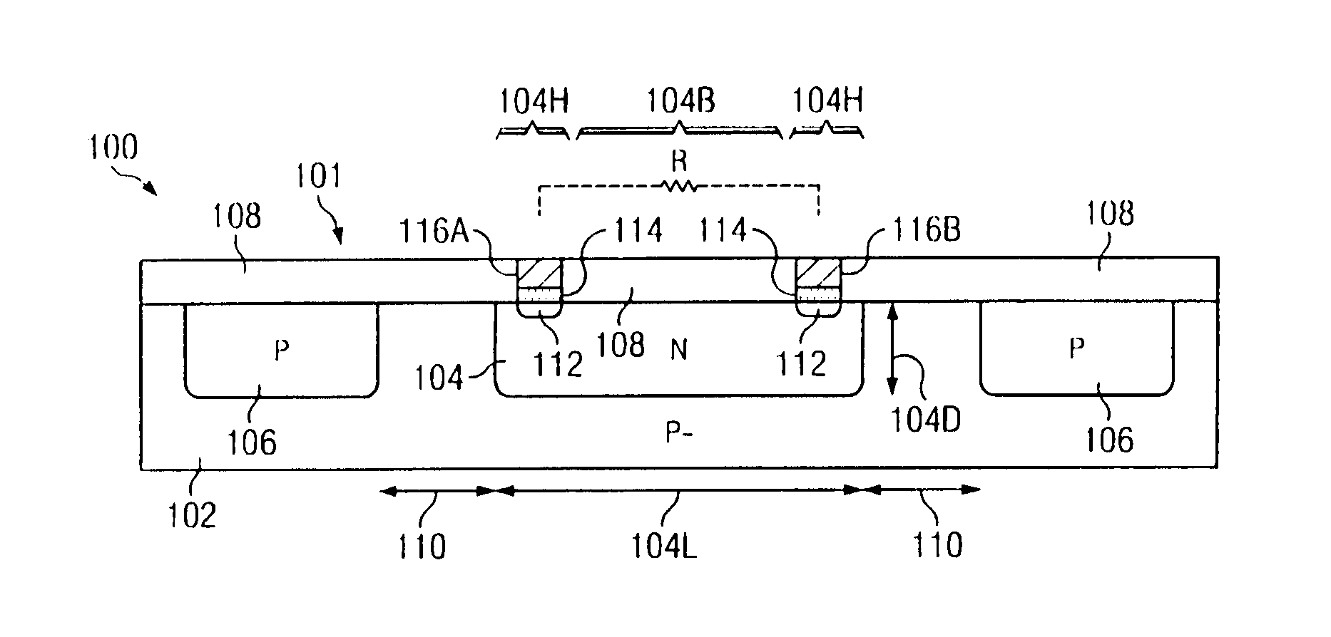
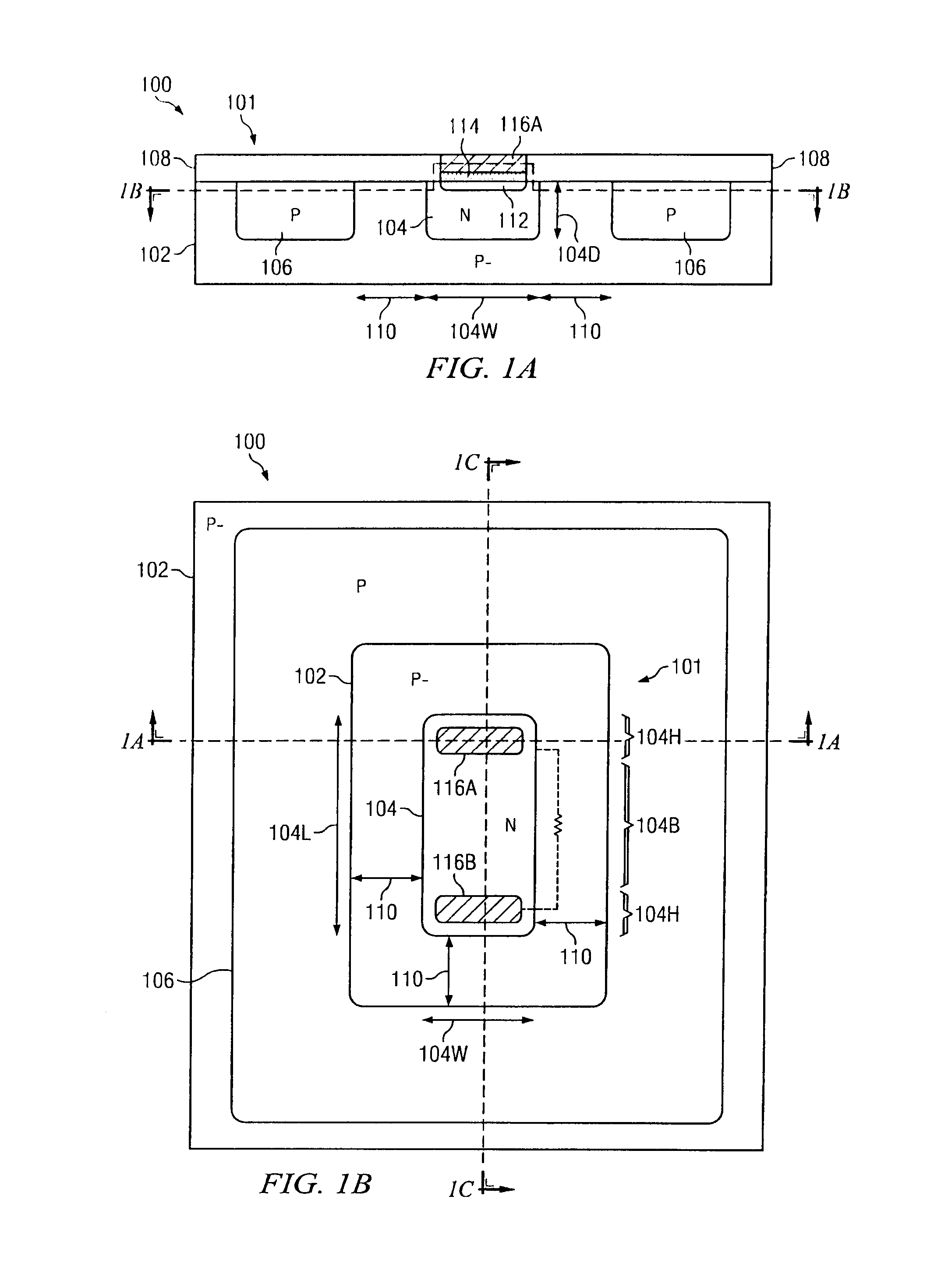
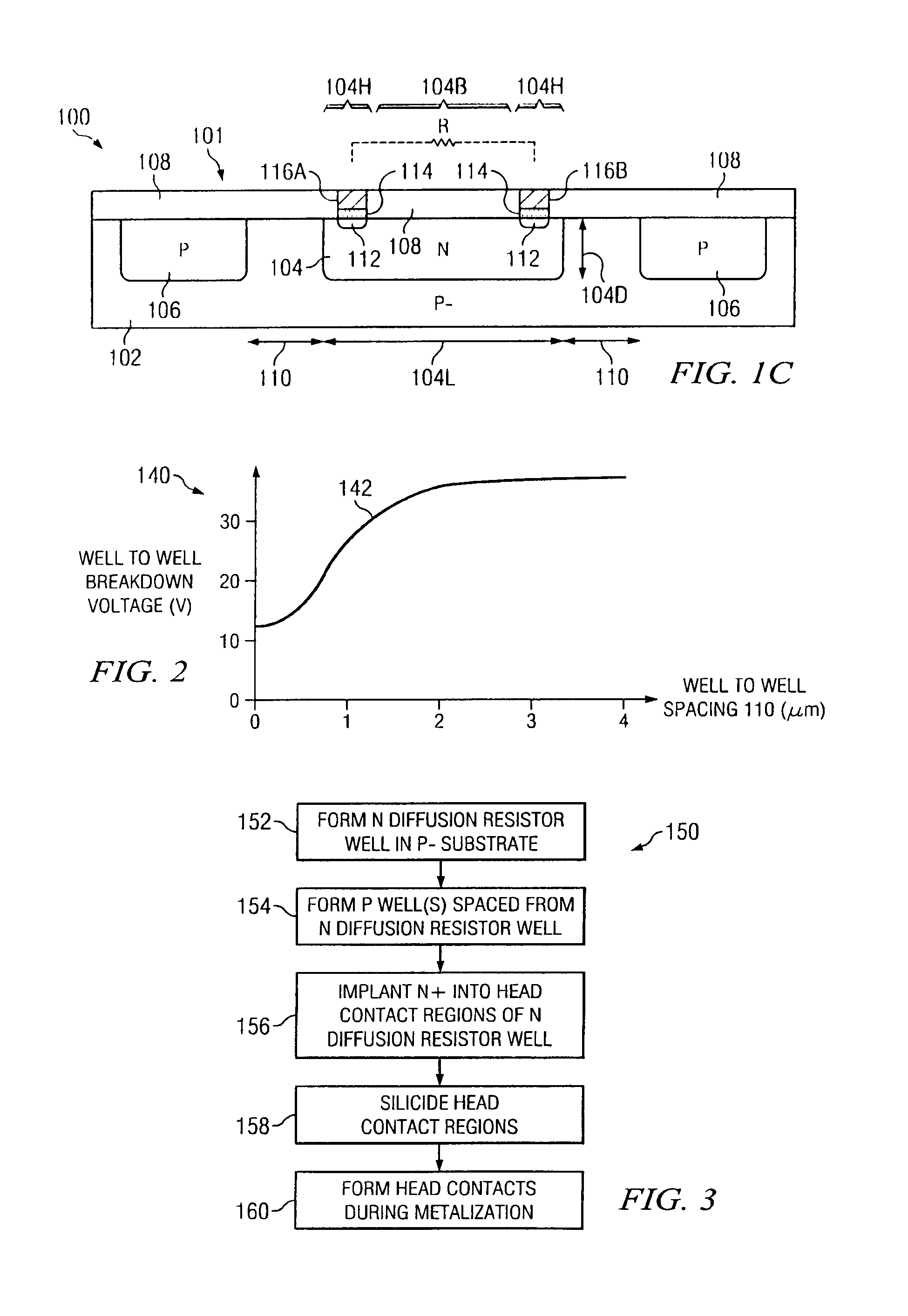
[0016]One or more embodiments or implementations are hereinafter described in conjunction with the drawings, wherein like reference numerals are used to refer to like or similar elements throughout. The various features are not necessarily drawn to scale and are provided merely to illustrate the various concepts of the present disclosure. Several aspects of the invention are described below with reference to example applications for illustration. It should be understood that numerous specific details, relationships, and methods are set forth to provide a full understanding of the disclosed concepts. One skilled in the relevant art, however, will readily recognize that these concepts can be practiced without one or more of the specific details or with other methods. In other instances, well-known structures or operations are not shown in detail to avoid obscuring the disclosed apparatus and processes, wherein the present disclosure is not limited by the illustrated ordering of acts o...


PUM

PropertyMeasurementUnit
depthaaaaaaaaaa
lateral spacing distanceaaaaaaaaaa

Abstract

Integrated circuits and manufacturing methods are presented for creating diffusion resistors (101, 103) in which the diffusion resistor well is spaced from oppositely doped wells to mitigate diffusion resistor well depletion under high biasing so as to provide reduced voltage coefficient of resistivity and increased breakdown voltage for high-voltage applications.

Description

FIELD OF THE INVENTION[0001]The present disclosure relates to the field of integrated circuits (ICs), and more particularly to diffusion resistors and methods for making the same.BACKGROUND OF THE INVENTION[0002]Diffusion resistors or well resistors are commonly implemented as nwell structures in P-substrate twin-well bulk CMOS technology surrounded by an adjacent pwell. These diffusion resistors, however, suffer from relatively low breakdown voltage (BV) and high voltage coefficient of resistivity (VCR) by which conventional diffusion resistors are typically unsuitable for high voltage applications. Alternative resistor structures may be used, such as silicided polysilicon resistors or silicide blocked polysilicon resistors. Polysilicon has a relatively low sheet resistance and these resistor structures are therefore larger than corresponding diffusion resistors for a given desired resistance value. For instance, typical diffusions may have a resistivity of about 500 ohms per squar...

Claims


Application Information

Patent Timeline
Patent Type & Authority Applications(United States)
IPC IPC(8): H01L29/06H01L21/761
CPCH01L29/8605H01L29/66166H01L27/0629H01L27/0802H01L21/266H01L21/823493H01L21/761
Inventor BENAISSA, KAMELCHATTERJEE, AMITAVA
Owner TEXAS INSTR INC
Why Eureka
Try Eureka