Pixel and organic light emitting display device using the same

a technology of light-emitting display device and pixel, which is applied in the direction of static indicating device, thermoelectric device, instrument, etc., can solve the problems of lowering the reliability of the circuit, improper threshold voltage compensation, and inability to compensate the threshold voltage during the period, so as to achieve stable compensation, simple circuit, and minimize leakage current

Inactive Publication Date: 2014-03-13
SAMSUNG DISPLAY CO LTD
View PDF6 Cites 5 Cited by
  • Summary
  • Abstract
  • Description
  • Claims
  • Application Information

AI Technical Summary

Benefits of technology

[0018]In the pixel and the organic light emitting display device according to the present invention, a diode-coupled driving transistor is turned on at the moment when the voltage of a gate electrode of the driving transistor is dropped to a voltage lower than that of a data signal. Thus, the voltage of the gate electrode of the driving transistor is not excessively dropped, and accordingly, the threshold voltage of the driving transistor can be stably compensated. Further, in the present invention, the gate electrode of the driving transistor is not directly coupled to a low power (e.g., an initialization power), and accordingly, leakage current can be minimized. Furthermore, in the present invention, it is possible to compensate for the threshold voltage of the driving transistor using a relatively simple circuit.

Problems solved by technology

However, in the organic light emitting display device, the amount of current that flows in an organic light emitting diode is changed depending on the variation in the threshold voltage of the driving transistor included in each pixel, and therefore, images with unequal luminance are displayed.
Practically, it is unlikely in the current fabrication process to fabricate the organic light emitting display device so that all transistors of the organic light emitting display device have the same characteristics.
However, in a case where the gate electrode of the driving transistor is initialized to a low voltage, the compensation of the threshold voltage is not properly made during the period of supplying the scan signal.
However, since the voltage of the gate electrode of the driving transistor is set to a low negative voltage, the compensation of the threshold voltage is not properly made in a high-resolution panel having a reduced period of supplying a scan signal and / or a panel driven at a high driving frequency.
Furthermore, since six transistors and two or more capacitors are usually included in a related art compensation circuit, the circuit is complicated, and accordingly, the reliability of the circuit is lowered.

Method used


Image

  • Pixel and organic light emitting display device using the same
  • Pixel and organic light emitting display device using the same
  • Pixel and organic light emitting display device using the same

Examples


first embodiment

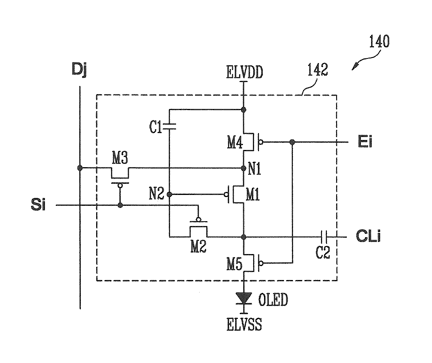
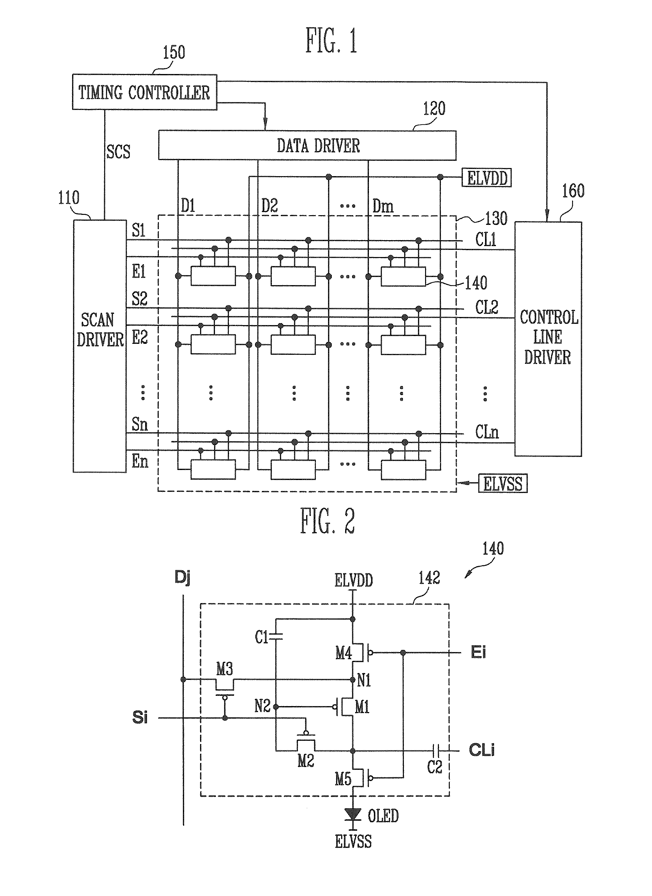
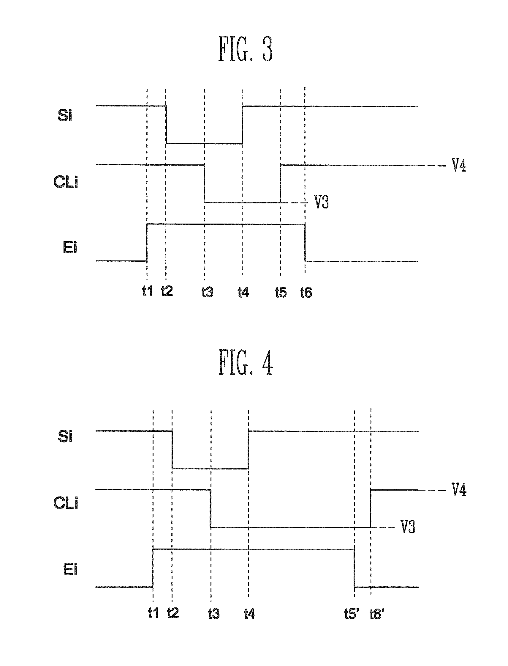
[0044]FIG. 3 is a waveform diagram illustrating driving waveforms according to the present invention.

[0045]Referring to FIG. 3, at time t1, a high-level emission control signal is first supplied to the emission control line Ei so that the fourth and fifth transistors M4 and M5 are turned off. If the fourth transistor M4 is turned off, the first power ELVDD and the first node N1 are electrically cut off. If the fifth transistor M5 is turned off, the first transistor M1 and the organic light emitting diode OLED are electrically cut off. Therefore, the organic light emitting diode OLED is set to be in a non-emission state during a period in which the high-level emission control signal is supplied to the emission control line Ei.

[0046]Then, at time t2, a low-level scan signal is supplied to the i-th scan line Si so that the third and second transistors M3 and M2 are turned on. If the second transistor M2 is turned on, the first transistor M1 is diode-coupled. If the third transistor M3 ...


PUM


Abstract

There are provided a pixel and an organic light emitting display device using the same capable of improving image quality. A pixel includes an organic light emitting diode, a first transistor, a second transistor and a second capacitor. The first transistor controls the amount of current supplied from a first power to the organic light emitting diode coupled to a second electrode of the first transistor, corresponding to a voltage applied to a second node. The second transistor is coupled between the second electrode of the first transistor and the second node so as to be turned on when a scan signal is supplied to a scan line. The second capacitor is coupled between the second electrode of the first transistor and a control line.

Description

CLAIM OF PRIORITY[0001]This application makes reference to, incorporates the same herein, and claims all benefits accruing under 35 U.S.C. §119 from an application earlier filed in the Korean Intellectual Property Office on Sep. 10, 2012 and there duly assigned Serial No. 10-2012-0100020.BACKGROUND OF THE INVENTION[0002]1. Field of Invention[0003]Embodiments of the present invention relate to a pixel and an organic light emitting display device using the same, and more particularly, to a pixel and an organic light emitting display device using the same capable of improving image quality.[0004]2. Description of the Related Art[0005]Recently, there have been developed various types of flat panel display devices capable of reducing the weight and volume of cathode ray tubes, which are disadvantages. The flat panel display devices include liquid crystal displays, field emission displays, plasma display panels, organic light emitting display devices, and the like.[0006]Among these flat p...

Claims


Application Information

Patent Timeline
Patent Type & Authority Applications(United States)
IPC IPC(8): G09G3/34H01L27/32
CPCH01L27/3225G09G3/34G09G3/3233G09G3/3291G09G2300/043G09G2300/0819G09G2300/0842G09G2300/0861G09G2300/0876G09G2320/045G09G3/30H10K59/00
Inventor ROH, JAE-DUKIM, YANG-WAN
Owner SAMSUNG DISPLAY CO LTD
Why Eureka
Try Eureka