Substrate bonding apparatus, substrate holding apparatus, substrate bonding method, substrate holding method, multilayered semiconductor device, and multilayered substrate

a technology of substrate holding and substrate, which is applied in the directions of transportation and packaging, semiconductor/solid-state device details, and other domestic articles. it can solve the problem that the substrates to be bonded together cannot be aligned to each other

Active Publication Date: 2014-03-13
NIKON CORP
View PDF4 Cites 38 Cited by
  • Summary
  • Abstract
  • Description
  • Claims
  • Application Information

AI Technical Summary

Benefits of technology

[0006]Therefore, it is an object of an aspect of the innovations herein to provide a substrate bonding apparatus, a substrate holding apparatus, a substrate bonding method, a substrate holding method, a multilayered semiconductor device and a multilayered substrate, which are capable of overcoming the above drawbacks accompanying the related art. The above and other objects can be achieved by combinations described in the claims. A first aspect of the innovations may include a substrate holding apparatus including a holder that holds a substrate to be bonded to another substrate, and a deformer that deforms the substrate held by the holder in a direction intersecting the surface of the held substrate in order to correct misalignment between the held substrate and the other substrate.

Problems solved by technology

Therefore, substrates to be bonded together cannot be aligned to each other simply by moving them relative to each other.

Method used


Image

  • Substrate bonding apparatus, substrate holding apparatus, substrate bonding method, substrate holding method, multilayered semiconductor device, and multilayered substrate
  • Substrate bonding apparatus, substrate holding apparatus, substrate bonding method, substrate holding method, multilayered semiconductor device, and multilayered substrate
  • Substrate bonding apparatus, substrate holding apparatus, substrate bonding method, substrate holding method, multilayered semiconductor device, and multilayered substrate

Examples


Embodiment Construction

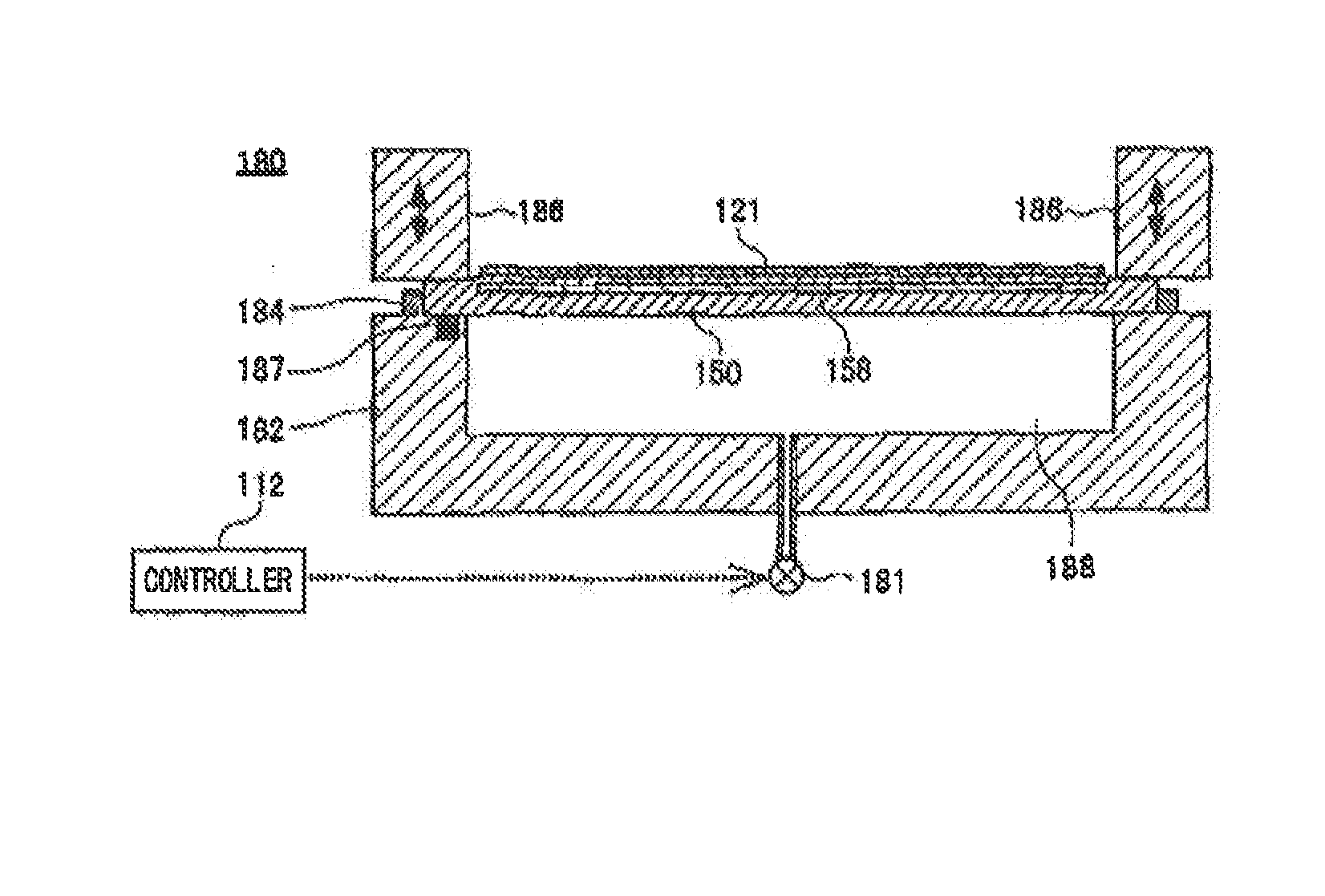
[0071]Hereinafter, some embodiments of the present invention will be described. The embodiments do not limit the invention according to the claims, and all the combinations of the features described in the embodiments are not necessarily essential to means provided by aspects of the invention.

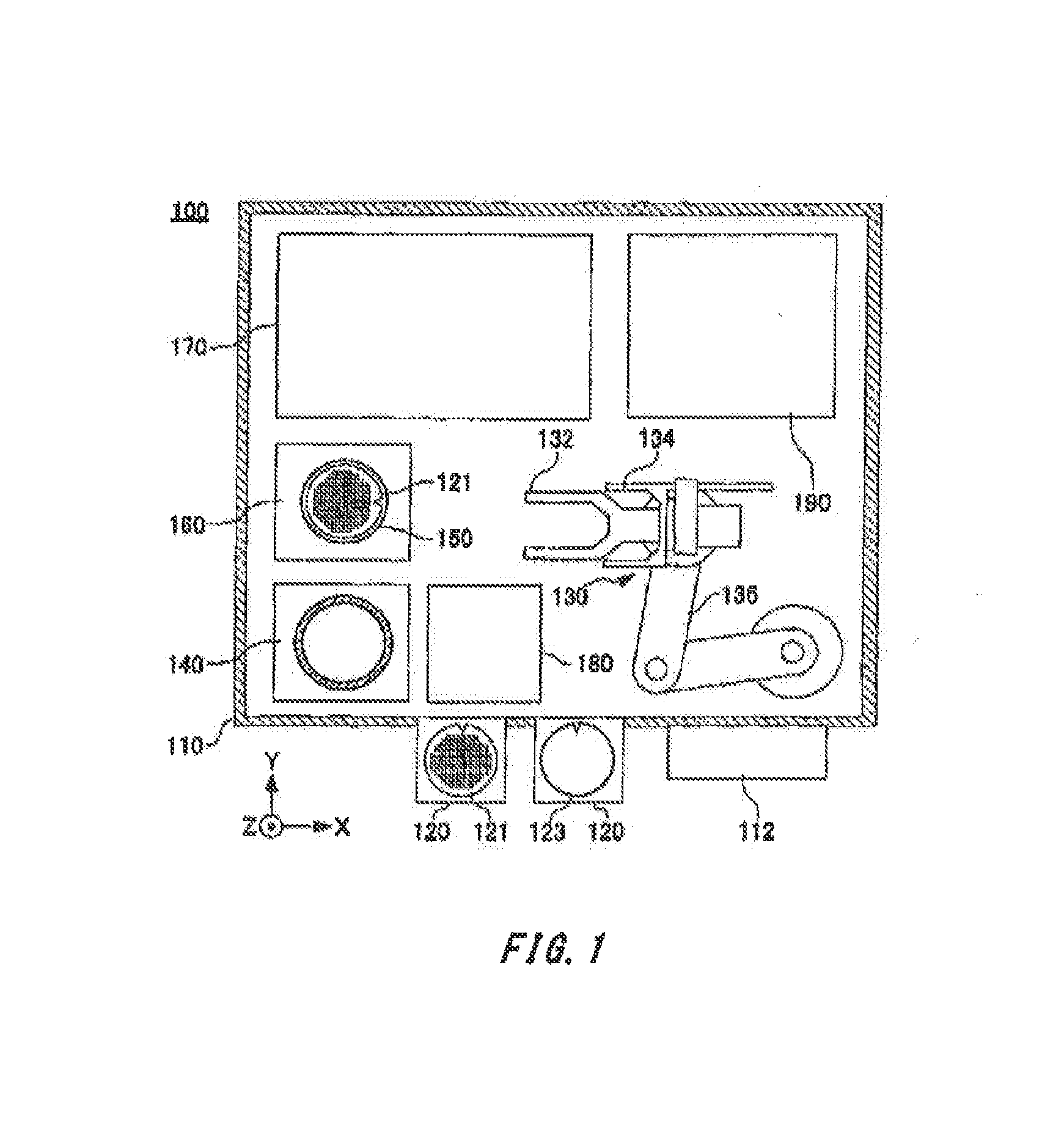
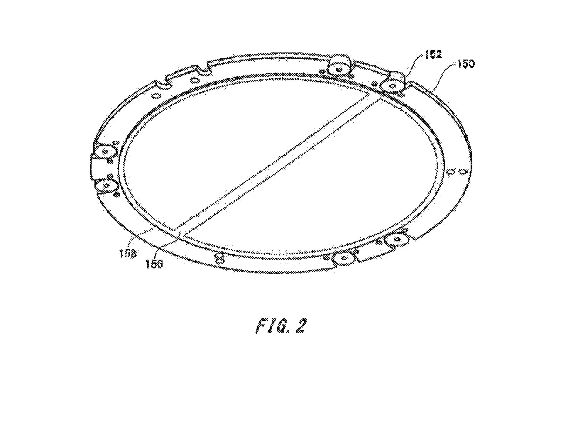
[0072]FIG. 1 is a schematic plan view of a multilayered substrate manufacturing apparatus 100. The multilayered substrate manufacturing apparatus 100 manufactures a multilayered substrate 123 by stacking a pair of substrates 121 onto each other.

[0073]The multilayered substrate manufacturing apparatus 100 includes a housing 110, a loader 130 housed within the housing 110, a holder stocker 140, a pre-aligner 160, an aligner 170, a bender 180 and a pressing apparatus 190. On the external surface of the housing 110, a controller 112 and a plurality of front opening unified pods (FOUPs) 120 are arranged.

[0074]The multilayered substrate manufacturing apparatus 100 further includes the controller 112....


PUM

PropertyMeasurementUnit
diameteraaaaaaaaaa
friction coefficientaaaaaaaaaa
voltageaaaaaaaaaa

Abstract

Substrates are aligned and then bonded to each other. A substrate bonding apparatus includes a deformer that deforms at least a first one of two substrates that are to be bonded to each other in order to correct misalignment between the two substrates, a holder that holds the deformed first substrate in the deformed state achieved by the deformer, a transporter that transports the holder from a position at which the deformed first substrate is held by the holder while the first substrate remains deformed, and a bonder that bonds the first substrate that has been transported by the transporter to the second substrate. In the above-described substrate bonding apparatus, while the first substrate is not held by the holder, the deformer may deform the holder from a first state to a second state that is more deformed than the first state, and while the first substrate is held by the holder, the deformer may reduce the amount of the deformation of the holder to less than the amount of the deformation of the second state to deform the first substrate.

Description

BACKGROUND[0001]1. Technical Field[0002]The present invention relates to a substrate bonding apparatus, a substrate holding apparatus, a substrate bonding method, a substrate holding method, a multilayered semiconductor device and a multilayered substrate.[0003]2. Related Art[0004]A known multilayered semiconductor device is provided by stacking and bonding a plurality of substrates onto each other (see Japanese Patent Application Publication No. 2005-251972). To bond a plurality of substrates together, the substrates are aligned to each other with high accuracy on the order of the line width of semiconductor devices.[0005]Referring to semiconductor device manufacturing process, parameters such as the magnification ratios of patterns transferred from masks and substrate flatness may be different globally or locally on substrates. Therefore, substrates to be bonded together cannot be aligned to each other simply by moving them relative to each other.SUMMARY[0006]Therefore, it is an o...

Claims


Application Information

Patent Timeline
Patent Type & Authority Applications(United States)
IPC IPC(8): B32B38/18H01L23/12
CPCH01L23/12B32B38/1833B32B37/0046B32B37/08B32B38/1841B32B38/1875B32B2307/208B32B2309/60B32B2457/14H01L21/2007H01L21/67092H01L21/67288H01L21/681H01L21/6838H01L21/68735H01L2924/0002Y10T156/1002Y10T428/24628H01L2924/00H01L21/20H01L21/677
Inventor KITO, YOSHIAKISHIRASU, HIROSHIYOSHIHASHI, MASAHIROYUKI, DAISUKESUZUKI, KAZUHIROSUGAYA, ISAO
Owner NIKON CORP
Why Eureka
Try Eureka