Wafer positioning systems and methods thereof

a positioning system and positioning system technology, applied in the field of wafer positioning systems, can solve the problems of shortened production period, less vacuum system resources, and less space in multi-process chambers

Inactive Publication Date: 2008-06-17
TAIWAN SEMICON MFG CO LTD
View PDF20 Cites 14 Cited by
  • Summary
  • Abstract
  • Description
  • Claims
  • Application Information

AI Technical Summary

Benefits of technology

[0009]An wafer positioning system comprises a wafer handling chamber with a vacuum sealable opening catching wafers. At least one processing chamber disposed adjacent to the wafer handling chamber has an opening catching wafers, sealed with a gate. A wafer transfer robot with a tray disposed in the wafer handling chamber transports wafers into the processing chambers. A signal receiver is disposed on the front end of the tray. When the tray passes below a wafer, the signal receiver detects wafer position, generating a wafer position signal. A control module receives the wafer position signal through the signal receiver and compares the wafer position signal with a predetermined position signal to correct any misalignment of the wafer.

Problems solved by technology

Multi-process chambers require less space, have a shortened production period, and consume less vacuum system resources.
Due to mechanical loss, the wafer transfer robot 28, however, may cause displacement of the wafer position and is incapable of accurate, wafer positioning in the processing chambers.
Such displacement may create process instability and malfunction of the vacuum clamp head.
Due to the vacuum state of the wafer handling chamber, the machine must stop product processing and break vacuum to conduct the maintenance, interrupting production and possibly damaging wafers.
Furthermore, if horizontally mis-positioned, the wafer transfer robot 28 may lose horizontal stability, thus generating vibration, further damaging wafers and the wafer carrier.

Method used


Image

  • Wafer positioning systems and methods thereof
  • Wafer positioning systems and methods thereof
  • Wafer positioning systems and methods thereof

Examples


Embodiment Construction

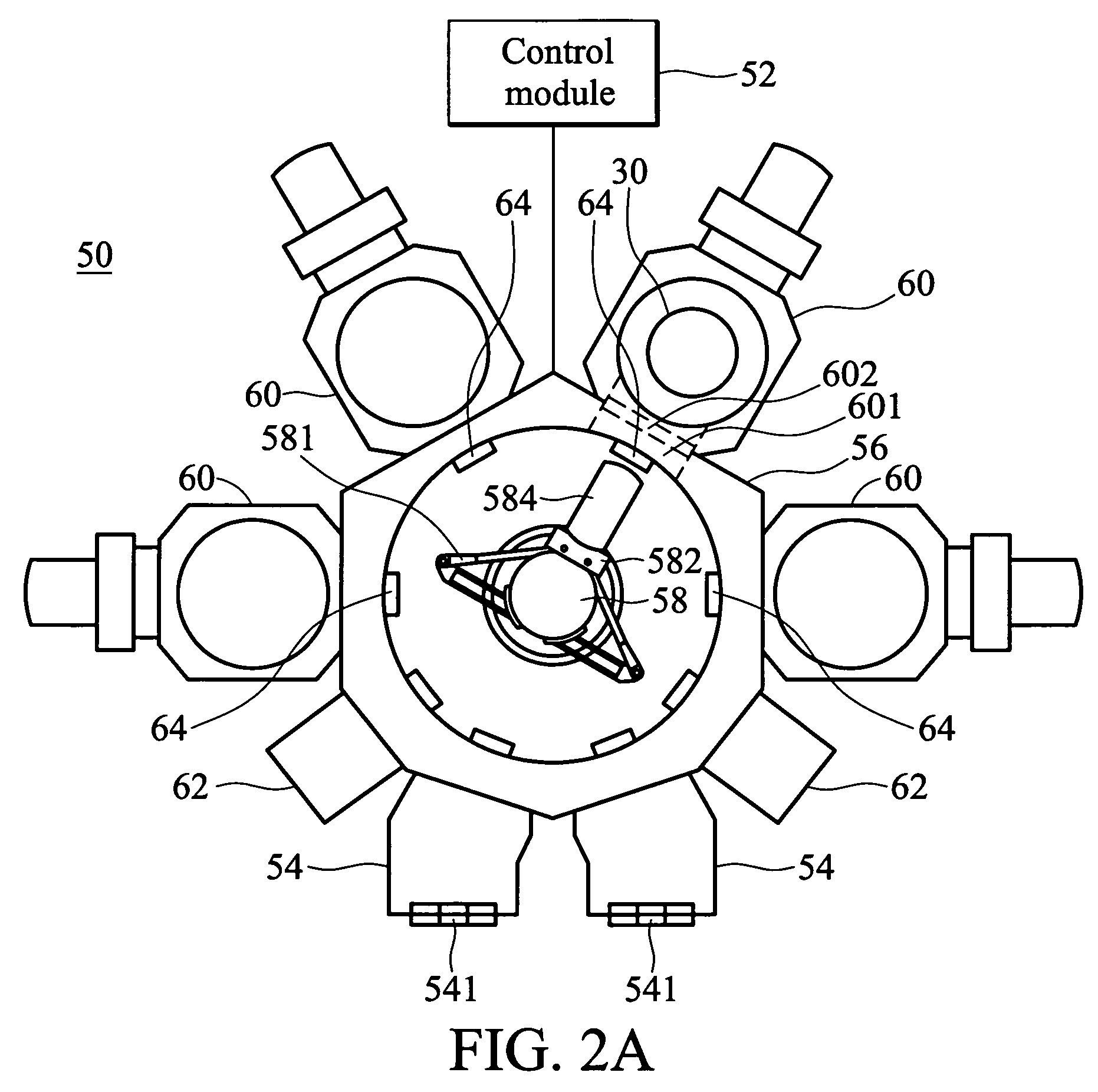
[0019]FIG. 2A is a diagram of a wafer positioning system and FIG. 2B shows a wafer transfer robot thereof catching a wafer. To simplify figures, a multi-process chamber 50 is shown in FIG. 2A&FIG. 2B without the front end wafer handling chamber and the wafer transfer robot in FIG. 1.

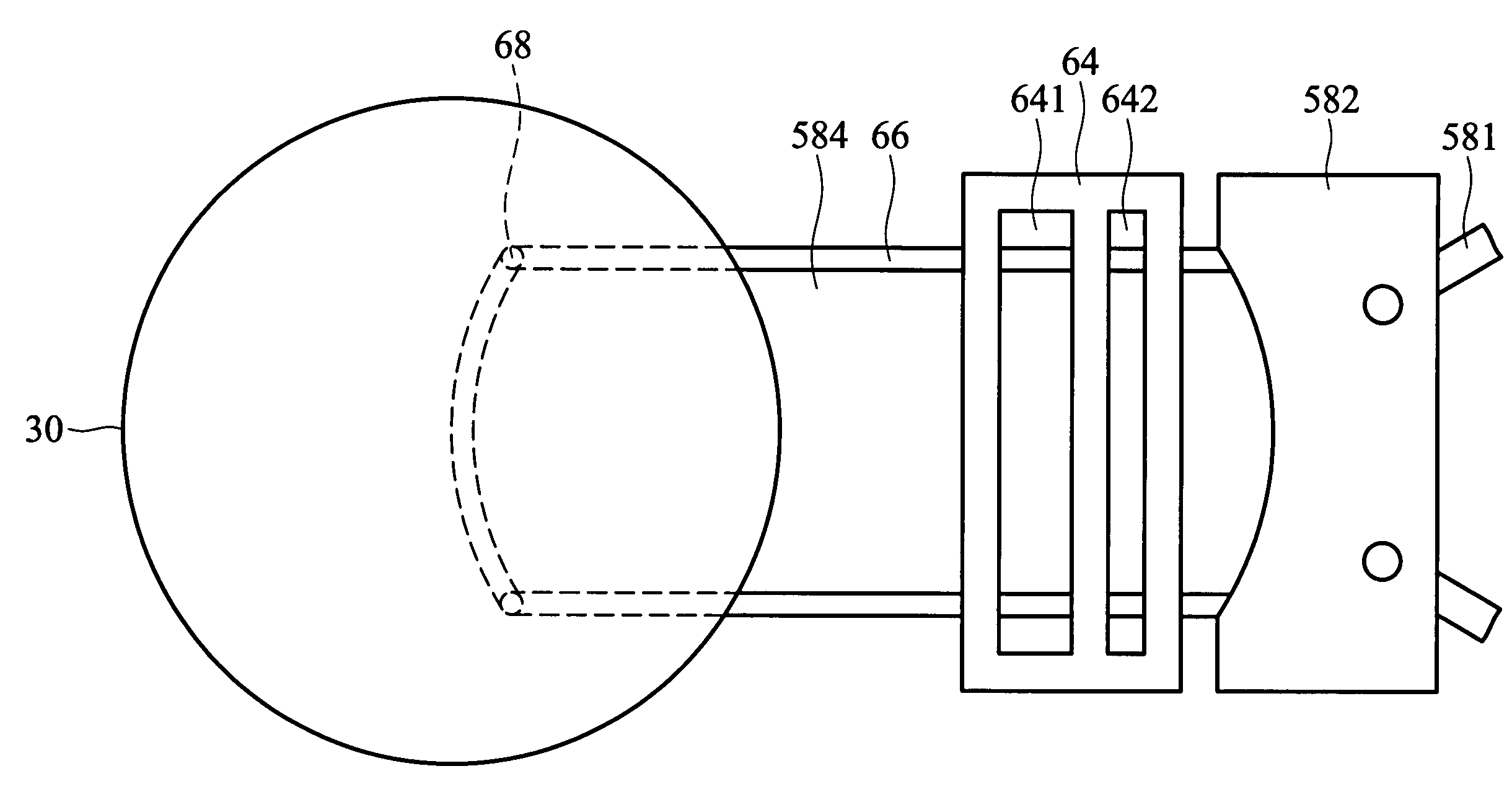
[0020]As shown in FIG. 2A&FIG. 2B, a multi-process chamber 50 comprises a wafer handling chamber 56 connected to the exterior via a vacuum chamber 54, sealed by a shutter 541. Outside the wafer handling chamber 56, a plurality of processing chambers 60 and cooling chambers 62 are disposed, each comprising a passage 601 and a gate 602. A wafer 30 enters the processing chamber 60 through the passage 601 and the gate 602 closes the passage 601. A wafer transfer robot 58, disposed to deliver the wafer 30, comprises a sub robot 581, a connection portion 582, and a tray 584 bearing the wafer 30. A control module 52 controls the system, e.g. the movement of the wafer transfer robot 58 and the process parameters...


PUM


Abstract

An wafer positioning system comprises a wafer handling chamber with a vacuum sealable opening catching wafers. At least one processing chamber disposed adjacent to the wafer handling chamber has an opening catching wafers, sealed with a gate. A wafer transfer robot with a tray disposed in the wafer handling chamber transports wafers into the processing chambers. A signal receiver is disposed on the front end of the tray. When the tray passes below a wafer, the signal receiver detects wafer position, generating a wafer position signal. A control module receives the wafer position signal through the signal receiver and compares the wafer position signal with a predetermined position signal to correct any misalignment of the wafer.

Description

BACKGROUND OF THE INVENTION[0001]1. Field of the Invention[0002]The invention relates to wafer positioning systems, and in particular to an on-line wafer positioning system having signal receiver to detect wafer position.[0003]2. Brief Discussion of the Related Art[0004]Semiconductor manufacturing processes include processes such as oxidation, diffusion, lithography, etching, CVD, and others. To integrate related processes in a single system and process and transfer wafers quickly in a vacuum environment avoiding contamination, automatic semiconductor manufacturing equipment is critical.[0005]Multi-process chambers require less space, have a shortened production period, and consume less vacuum system resources. A general multi-process chamber design, as shown in FIG. 1, comprises a front end wafer handling chamber 14 connecting the transfer system of the factory and transferring wafer carriers to a load lock chamber 16 via robots 18. Further, a wafer handling chamber 20 is disposed ...

Claims


Application Information

Patent Timeline
Patent Type & Authority Patents(United States)
IPC IPC(8): B65G49/07
CPCH01L21/67167H01L21/67265H01L21/67748Y10S414/139
Inventor HO, CHIH-CHIENSHIEH, JENN-SHIANG
Owner TAIWAN SEMICON MFG CO LTD
Why Eureka
Try Eureka