Programmable physical address mapping for memory

Active Publication Date: 2014-03-20
ADVANCED MICRO DEVICES INC
View PDF9 Cites 29 Cited by
  • Summary
  • Abstract
  • Description
  • Claims
  • Application Information

AI Technical Summary

Problems solved by technology

However, this approach requires software modifications in the operating system, compiler, or runtime software, as welt as requiring the software designer to have foreknowledge of both the likely access pattern for the data and the memory address redirection needed to optimize the access pattern.
Moreover, this approach only benefits those software applications specifically designed and compiled in this manner.

Method used


Image

  • Programmable physical address mapping for memory
  • Programmable physical address mapping for memory
  • Programmable physical address mapping for memory

Examples


Embodiment Construction

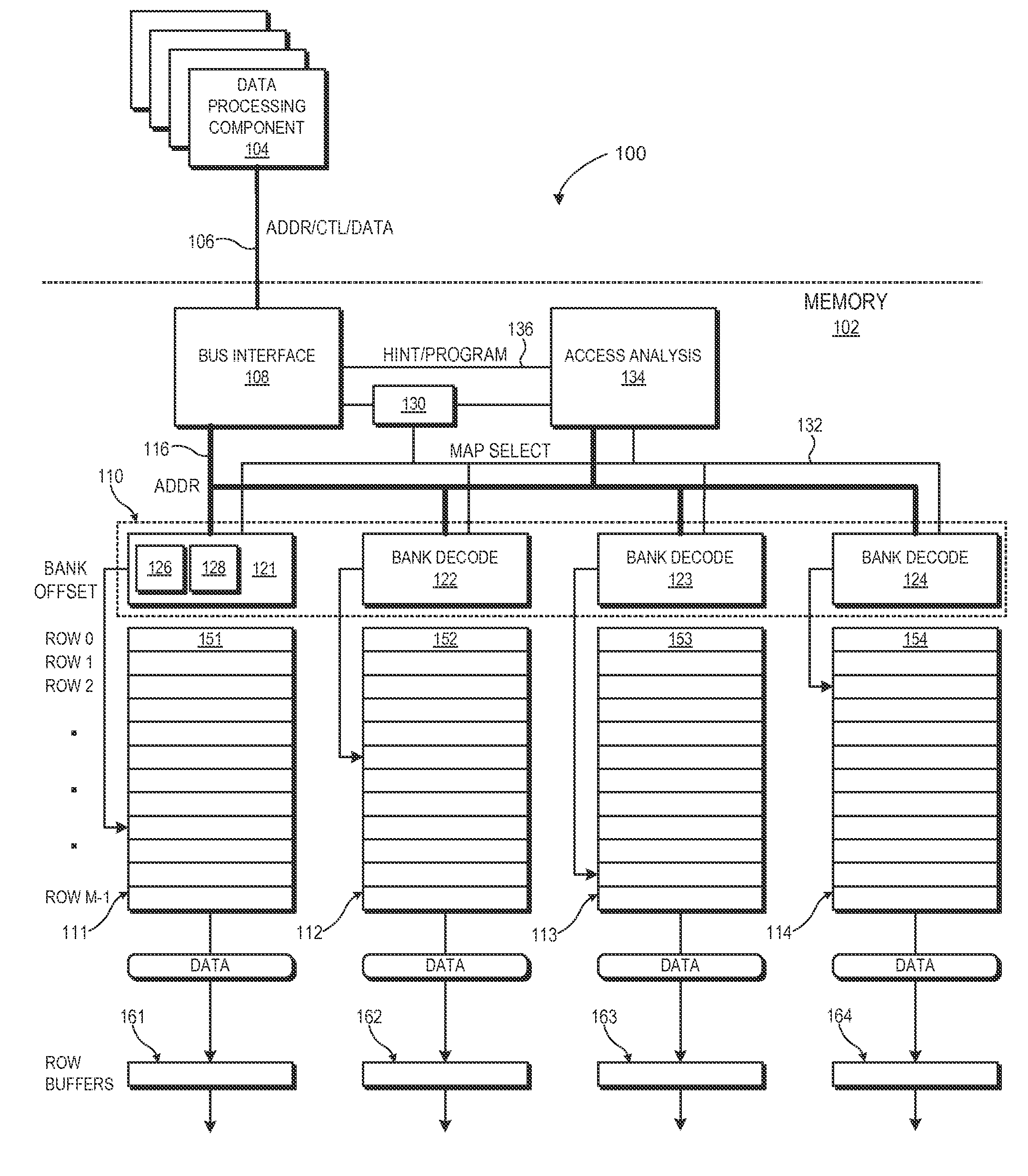
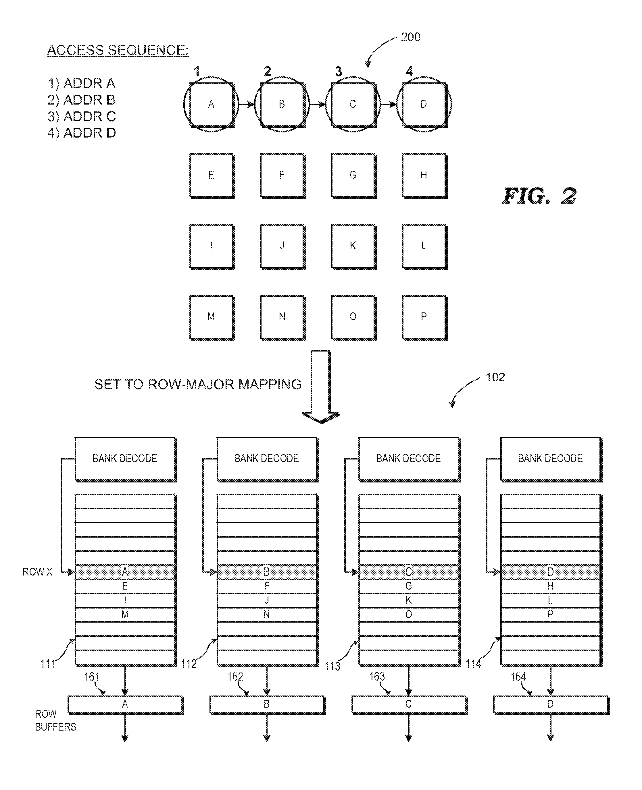
[0014]FIGS. 1-8 illustrate example implementations of a multiple-bank memory having a programmable physical address mapping so as to enable the mapping of physical addresses to banks and rows to change to reflect changing access patterns, observed or anticipated, to the memory. In some embodiments, the memory employs address decode logic that can implement any of a variety of physical address mappings between physical addresses and corresponding memory locations. The physical address mappings may locate the data within the banks and rows of the memory so as to facilitate more efficient memory accesses for a given access pattern. For example, because dynamic random access memory (DRAM)-based architectures often incur an access penalty when different rows of the same bank are accessed in sequence, the physical address mapping may place data expected to be accessed in sequence in the same row across multiple banks, thereby reducing or avoiding this access penalty. The programmable phys...


PUM


Abstract

A memory implements a programmable physical address mapping that can change to reflect changing memory access patterns, observed or anticipated, to the memory. The memory employs address decode logic that can implement any of a variety of physical address mappings between physical addresses and corresponding memory locations. The physical address mappings may locate the data within one or more banks and rows of the memory so as to facilitate more efficient memory accesses for a given access pattern. The programmable physical address mapping employed by the hardware of the memory can include, but is not limited to, hardwired logic gates, programmable look-up tables or other mapping tables, reconfigurable logic, or combinations thereof. The physical address mapping may be programmed for the entire memory or on a per-memory region basis.

Description

BACKGROUND[0001]1. Field of the Disclosure[0002]The present disclosure generally relates to memory, and, more particularly, to mapping of physical addresses to memory locations in a memory with one or more banks.[0003]2. Description of the Related Art[0004]Many memory architectures are organized into one or more banks, both at the structural level and the silicon implementation level. Typically, a physical address is uniquely mapped to a corresponding row of a corresponding bank. The mapping of physical addresses to corresponding bank / row locations generally is selected at design time and remains fixed. Certain memory architectures, such as dynamic random access memory (DRAM)-based architectures and phase change memory architectures, have certain set-up requirements that cause successive accesses to different rows of the same bank to take considerably longer than successive accesses to the same row. Further, some memory architectures utilize a row buffer to buffer data at an activat...

Claims


Application Information

Patent Timeline
Patent Type & Authority Applications(United States)
IPC IPC(8): G06F12/00
CPCG06F12/0653G06F12/0207G06F2212/1016G06F12/00
Inventor LOH, GABRIEL H.BRETERNITZ, JR., MAURICIO
Owner ADVANCED MICRO DEVICES INC
Why Eureka
Try Eureka