Light-Emitting Element

a technology of light-emitting elements and energy transfer, which is applied in the field of light-emitting elements, can solve the problems of increasing drive voltage, reducing power efficiency, and insufficient utilization of energy transfer from the singlet excited state of the host to the guest, and achieves the effects of low power consumption, high emission efficiency, and reduced barrier to carrier injection

Inactive Publication Date: 2014-03-27
SEMICON ENERGY LAB CO LTD
View PDF8 Cites 60 Cited by
  • Summary
  • Abstract
  • Description
  • Claims
  • Application Information

AI Technical Summary

Benefits of technology

[0036]An exciplex probably has an extremely small difference between the singlet excitation energy and the triplet excitation energy. In other words, the emission from the singlet state of the exciplex and that from the triplet state of the exciplex appear in wavelength regions which are very close to each other. In addition, because emission of an exciplex is usually observed on the longer wavelength side than that of its monomer state, the overlap between the absorptions of phosphorescent compounds, which appear in a long wavelength region and originate from the triplet MLCT transition, and the emission of the exciplex can be large. This means that energy can be efficiently transferred from both of the singlet and triplet states of the exciplex to the phosphorescent compounds, which contributes to the improvement in the emission efficiency of the light-emitting elements.
[0052]The light-emitting element of one embodiment of the present invention includes the layer containing the p-type host, the light-emitting layer containing the guest, the p-type host, and the n-type host, and the layer containing the n-type host. Since the combination of the p-type host and the n-type host forms an exciplex, one embodiment of the present invention not only enables confinement of carriers and a reduction in a barrier to carrier injection into the light-emitting layer but also allows formation of an exciplex and the utilization of the energy transfer process from both of the singlet and triplet excited states of the exciplex; thus, a light-emitting element with high emission efficiency can be obtained.

Problems solved by technology

Therefore, it is impossible to sufficiently utilize the energy transfer from the singlet excited state of the host to the guest.
It is known that in the case where a light-emitting element has a junction of different layers, an energy gap generated at the interface causes an increase in drive voltage and a decrease in power efficiency (see Patent Document 2).

Method used


Image

  • Light-Emitting Element
  • Light-Emitting Element
  • Light-Emitting Element

Examples


embodiment 1

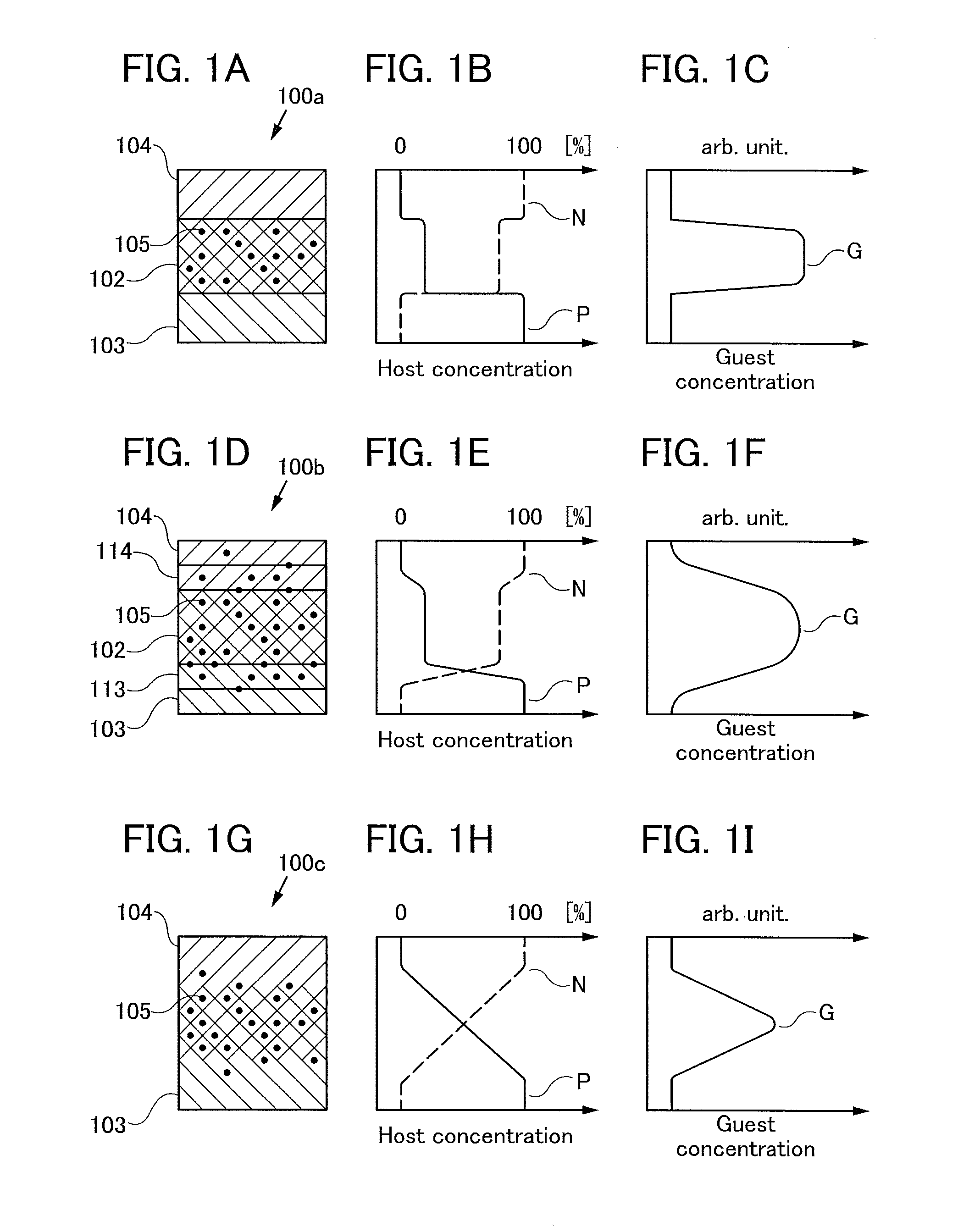
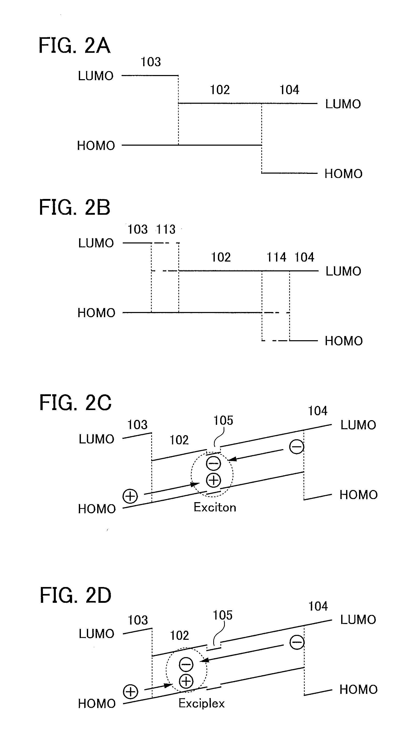
[0078]In this embodiment, a light-emitting element of one embodiment of the present invention will be described with reference to FIGS. 1A to 1I and FIGS. 2A to 2D.

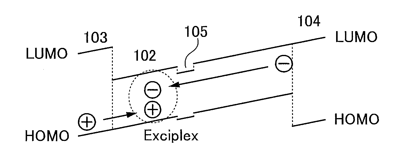
[0079]A light-emitting element of one embodiment of the present invention includes a layer (an EL layer) containing a light-emitting organic compound between a pair of electrodes (a first electrode and a second electrode). One of the pair of electrodes functions as an anode and the other functions as a cathode. The EL layer includes a first layer over the first electrode, a light-emitting layer over the first layer, and a second layer over the light-emitting layer. The light-emitting layer contains a phosphorescent compound (a guest), a first organic compound, and a second organic compound, where the content of the second organic compound is the highest. The first layer contains the first organic compound and does not contain the second organic compound. The second layer contains the second organic compound and does not c...

embodiment 2

[0140]In this embodiment, a light-emitting element of one embodiment of the present invention will be described with reference to FIGS. 3A to 3D.

[0141]The light-emitting element of this embodiment includes an EL layer between a pair of electrodes (an anode and a cathode).

[0142]A light-emitting element illustrated in FIG. 3A includes only a stack 100 as an EL layer between an anode 101 and a cathode 109. Any of the stacks 100a to 100c described in Embodiment 1 may be applied to the stack 100 in this embodiment. Note that in each of the stacks, the layer 103 containing the p-type host is provided on the anode 101 side and the layer 104 containing the n-type host is provided on the cathode 109 side. At least one of the anode 101 and the cathode 109 has a property of transmitting visible light.

[0143]In the stack 100 of the light-emitting element illustrated in FIG. 3A, the layer 103 containing the p-type host functions as a hole-transport layer and blocks electrons. Further, the layer 1...

embodiment 3

[0182]In this embodiment, apparatuses for manufacturing a light-emitting element of one embodiment of the present invention will be described with reference to FIGS. 4A to 4C.

[0183]A manufacturing apparatus illustrated in FIG. 4A includes a first deposition material holding portion 202, a second deposition material holding portion 203, and a third deposition material holding portion 204 in a vacuum chamber 201. The deposition material holding portions described in this embodiment each have a linear opening portion (see a linear opening portion 223 of the first deposition material holding portion 202 which is illustrated in FIG. 4C) and can be used to evaporate a deposition material therein by a resistance heating method.

[0184]In this embodiment, the first deposition material holding portion 202, the second deposition material holding portion 203, and the third deposition material holding portion 204 cause the p-type host, the guest, and the n-type host to evaporate, respectively. Th...


PUM


Abstract

A light-emitting element with high emission efficiency is provided. The light-emitting element includes, between a pair of electrodes, a layer containing a p-type host, a light-emitting layer containing a guest, the p-type host, and an n-type host, and a layer containing the n-type host. A combination of the p-type host and the n-type host forms an exciplex. Among the layer containing the p-type host, the light-emitting layer, and the layer containing the n-type host, the light-emitting layer has the highest secondary ion intensity of the n-type host, the layer containing the n-type host has the second-highest secondary ion intensity of the n-type host, and the layer containing the p-type host has the lowest secondary ion intensity of the n-type host in analysis by a time-of-flight secondary ion mass spectrometer.

Description

BACKGROUND OF THE INVENTION[0001]1. Field of the Invention[0002]The present invention relates to light-emitting elements using an organic electroluminescence (EL) phenomenon (hereinafter such light-emitting elements are also referred to as organic EL elements).[0003]2. Description of the Related Art[0004]Organic EL elements have been actively researched and developed. In a fundamental structure of the organic EL element, a layer (hereinafter also referred to as a light-emitting layer) containing an organic compound that is a light-emitting substance is provided between a pair of electrodes. The organic EL element has attracted attention as a next-generation flat panel display element owing to characteristics such as feasibility of being thinner and lighter, high speed response to input signals, and capability of direct current low voltage driving. In addition, a display using such an organic EL element has a feature that it is excellent in contrast and image quality, and has a wide ...

Claims


Application Information

Patent Timeline
Patent Type & Authority Applications(United States)
IPC IPC(8): H01L51/50
CPCH01L51/5016H01L51/5004H10K30/865H10K50/11H10K2101/40H10K2101/10H10K2101/90H10K50/135H10K50/805
Inventor YAMAZAKI, SHUNPEISEO, SATOSHISHITAGAKI, SATOKOOHSAWA, NOBUHARUINOUE, HIDEKOKADOMA, HIROSHIOSAKA, HARUE
Owner SEMICON ENERGY LAB CO LTD
Why Eureka
Try Eureka