Low-noise magnetic sensors

Active Publication Date: 2014-03-27
KING ABDULLAH UNIV OF SCI & TECH
View PDF6 Cites 3 Cited by
  • Summary
  • Abstract
  • Description
  • Claims
  • Application Information

AI Technical Summary

Benefits of technology

[0006]EMR is a large magnetoresistance effect that may arise in a nonmagnetic semiconductor metal hybrid structure. In an EMR effect sensor, the Lorentz force induced by a magnetic field may cause a redistribution of the electric current density between adjacent semiconductor and metal layers resulting in resistance changes. The EMR effect may be described by equation (1):
[0007]The dimensions of an EMR sensor, the thickness of its layers, and the placement of the voltage and current leads may significantly effect magnitude of the measured EMR. FIG. 1A and FIG. 1B depict prior art EMR effect sensors 100A and 100B. As depicted in both figures, EMR effect sensors 100A and 100B each have a metal layer 102 and a semiconductor layer 104. In both pictures, the voltage and current leads are arranged symmetrically around center 110 of the EMR effect sensor.
[0008]Voltage leads 106 and current leads 108 are located on one side of the device—coupled to semiconductor layer 104. FIG. 1A depicts voltage leads 106 and current leads 108 in an V-I-I-V formation, and FIG. 2A depicts the voltage and current in a I-V-V-I formation. The voltage (V) between voltage leads 106 and the current (I) through current leads 108 allow for the calculation of the resistance R(H) in equation (1) by using equation (2):
[0009]EMR effect sensors 100A and 100B can further be described by width 112 of the metal layer 102, width 114 of the semiconductor layer 104, and length 116 of the EMR effect sensor. FIG. 2 illustrates the simulated EMR effect for EMR effect sensor 1

Problems solved by technology

In an EMR effect sensor, the Lorentz force induced by a magnetic field may cause a redistribution of the

Method used


Image

  • Low-noise magnetic sensors
  • Low-noise magnetic sensors
  • Low-noise magnetic sensors

Examples


Example

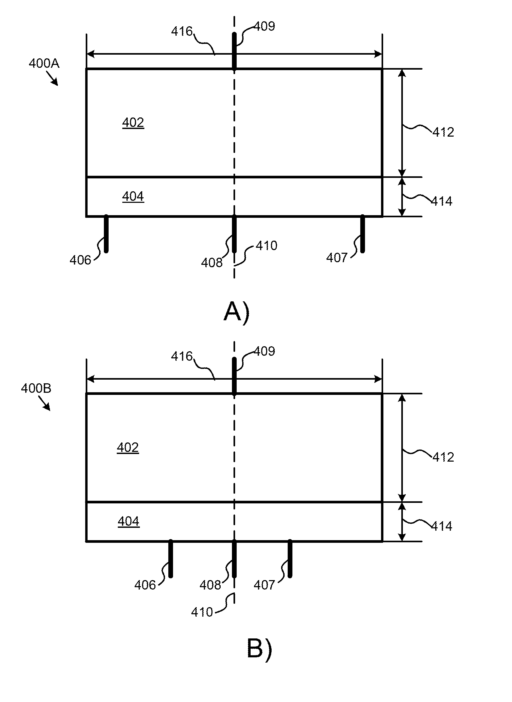
[0062]The present embodiments describe an advantageous structure that may be useful for sensing magnetic fields. Advantageously, the same or similar structure may be used for both an EMR sensor and a Hall Effect sensor. For example, embodiments of a semiconductor / metal hybrid structure, which comprises a conductive semiconductor layer and a metallic shunt are described. Another advantage of this structure may be the low-noise performance characteristics achieved through use of the hybrid metallic shunt structure, which may reduce the output resistance of the sensor.

[0063]In one embodiment, the magnetic sensor includes a semiconductor layer. In some embodiments, the sensor may include a conductive layer substantially coupled to the semiconductor layer. In some embodiments, the sensor may include a first voltage lead coupled to the semiconductor layer. In some embodiments, the first voltage lead may be configured to provide a voltage for measurement by a voltage measurement circuit. I...


PUM


Abstract

Magnetic sensors are disclosed, as well as methods for fabricating and using the same. In some embodiments, an EMR effect sensor includes a semiconductor layer. In some embodiments, the EMR effect sensor may include a conductive layer substantially coupled to the semiconductor layer. In some embodiments, the EMR effect sensor may include a voltage lead coupled to the conductive layer. In some embodiments, the voltage lead may be configured to provide a voltage for measurement by a voltage measurement circuit. In some embodiments, the EMR effect sensor may include a second voltage lead coupled to the semiconductor layer. In some embodiments, the second voltage lead may be configured to provide a voltage for measurement by a voltage measurement circuit. Embodiments of a Hall effect sensor having the same or similar structure are also disclosed.

Description

CROSS-REFERENCE TO RELATED APPLICATIONS[0001]This application is a continuation-in-part (CIP) to U.S. patent application Ser. No. 13 / 187,329 filed on Jul. 20, 2011, and claims priority to U.S. Provisional Application No. 61 / 733,973 filed Dec. 6, 2012, the entire contents of which are specifically incorporated herein by reference.BACKGROUND OF THE INVENTION[0002]1. Field of the Invention[0003]The present invention relates generally to magnetic sensors, more particularly, to extraordinary magnetoresistance (EMR) effect and Hall effect sensors and methods for making and using the same.[0004]2. Description of the Related Art[0005]Generally, there are at least two types of magnetic sensors that can be used to measure a magnetic field, including an EMR sensor and a Hall sensor. An EMR sensor operates based on an EMR effect. Broadly speaking, the EMR effect quantifies scattering of electrons at a material interface when an electric current is applied to the material. The scattering occurs ...

Claims


Application Information

Patent Timeline
IPC IPC(8): G01R33/09H01L43/02G01R33/07
CPCG01R33/095H01L43/02G01R33/07G01R33/0052G01R33/072H10N50/80
Inventor KOSEL, JURGENSUN, JIAN
Owner KING ABDULLAH UNIV OF SCI & TECH
Why Eureka
Try Eureka