Encapsulating sheet-covered semiconductor element, producing method thereof, semiconductor device, and producing method thereof

a technology of encapsulating sheet and semiconductor elements, which is applied in the direction of synthetic resin layered products, other domestic articles, chemistry apparatus and processes, etc., can solve the problems of reducing the reliability of the semiconductor device and easily generating voids in the resin, and achieves excellent reliability and easy steps

Active Publication Date: 2014-04-03
EPISTAR CORP
View PDF6 Cites 15 Cited by
  • Summary
  • Abstract
  • Description
  • Claims
  • Application Information

AI Technical Summary

Benefits of technology

[0027]In the method for producing a semiconductor device of the present invention, the encapsulating sheet-covered semiconductor element is prepared by the method for producing an encapsulating sheet-covered semiconductor element including the simplified encapsulating sheet disposing step, so that the semiconductor device is capable of being obtained by easy steps.
[0028]In the encapsulating sheet-covered semiconductor element of the present invention obtained by the method for producing an encapsulating sheet-covered semiconductor element of the present invention, the generation of a void in the encapsulating sheet is suppressed, so that the method for producing a semiconductor device of the present invention and the semiconductor device of the present invention obtained by the method have excellent reliability.

Problems solved by technology

Thus, there is a disadvantage that a bubble is easily involved (easily contained) therein and therefore, a void is easily generated in the resin.
As a result, the reliability of the semiconductor device is reduced.

Method used


Image

  • Encapsulating sheet-covered semiconductor element, producing method thereof, semiconductor device, and producing method thereof
  • Encapsulating sheet-covered semiconductor element, producing method thereof, semiconductor device, and producing method thereof
  • Encapsulating sheet-covered semiconductor element, producing method thereof, semiconductor device, and producing method thereof

Examples


first embodiment

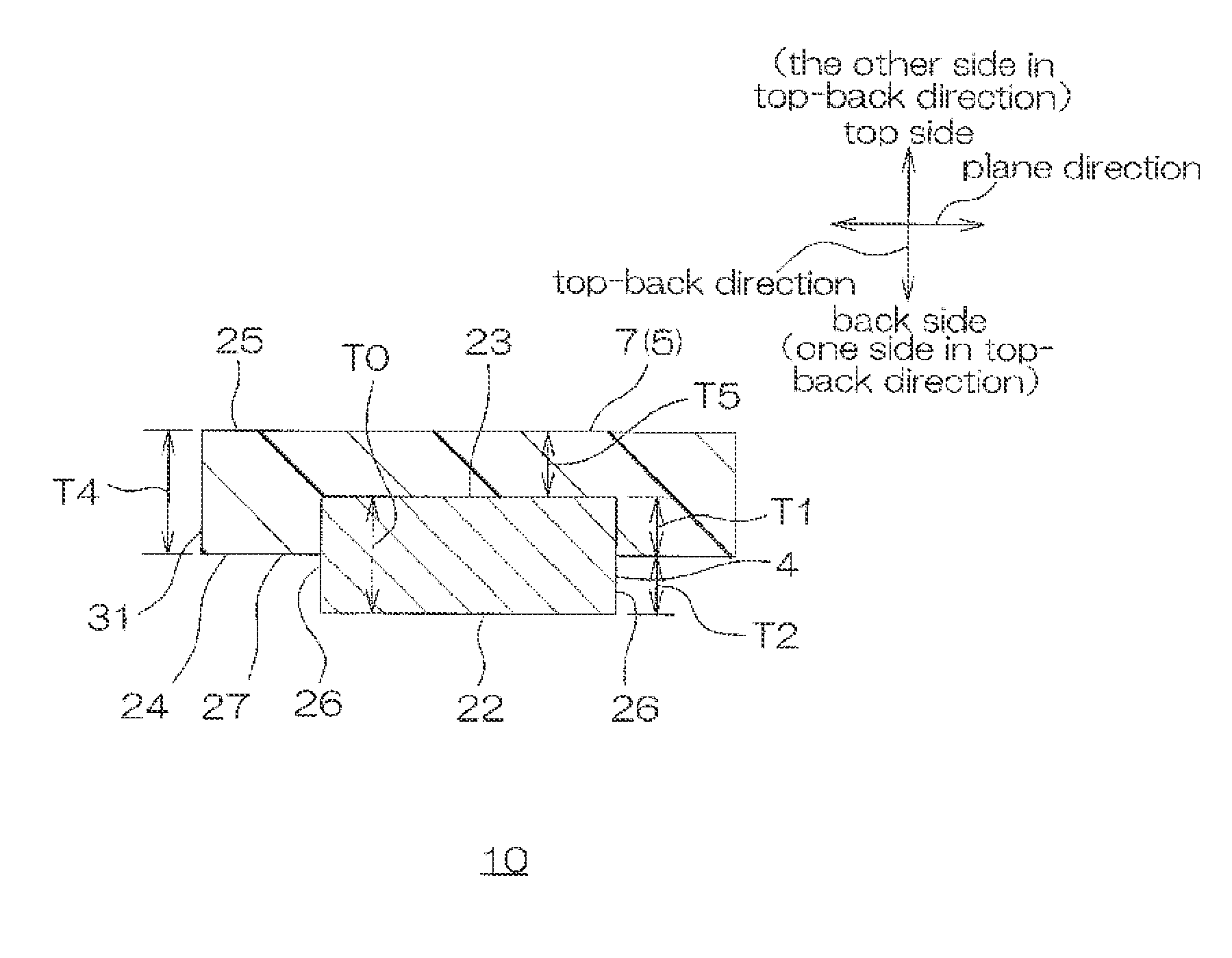
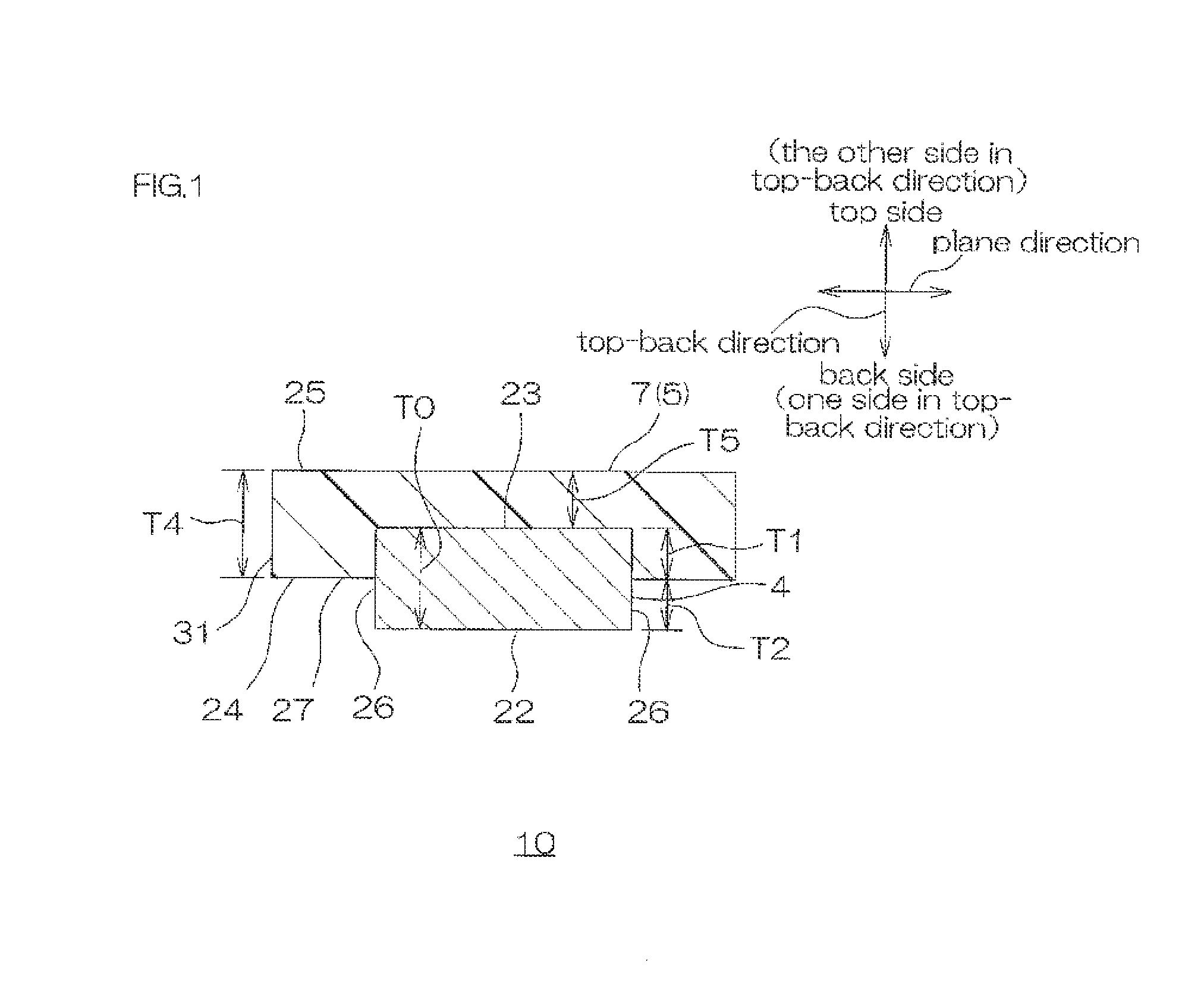
[0132]In FIG. 1, the up-down direction of the paper surface may be referred to as a first direction (a top-back direction); the depth direction of the paper surface may be referred to as a second direction (a front-rear direction); and the right-left direction of the paper surface may be referred to as a third direction. The top-back direction is a two-way direction of a direction going from the top surface that is the other surface to the back surface that is one surface and a direction going from the back surface to the top surface in an LED 4 to be described later. Furthermore, the direction going from the top surface to the back surface is defined as one side in the top-back direction and the direction going from the back surface to the top surface is defined as the other side in the top-back direction. Directions in FIG. 2 and the subsequent figures are in conformity with the directions in FIG. 1. In FIGS. 3, 6, and 12, a pressure-sensitive adhesive layer 3 to be described late...

second embodiment

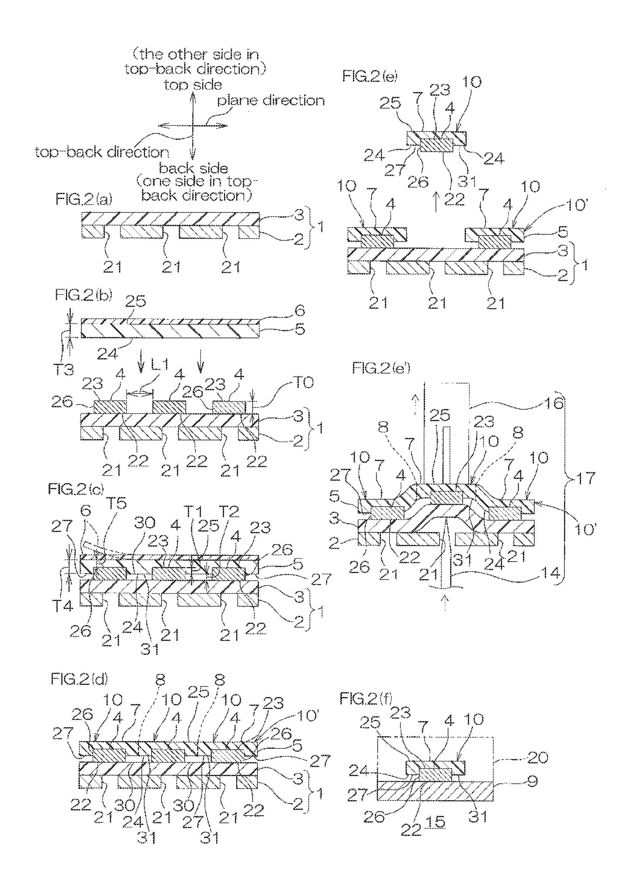
[0319]In FIGS. 11 and 12, the same reference numerals are provided for members and steps corresponding to each of those in the first embodiment, and their detailed description is omitted.

[0320]In the first embodiment, the through holes 21 are provided in the support board 2. Alternatively, for example, as shown in FIGS. 11 (a) and 12, the support board 2 can be formed into a flat plate shape having no through hole 21.

[0321]As shown in FIGS. 11 (a) to 11 (e), the method for producing the phosphor layer-covered LED 10 in the second embodiment includes a support sheet preparing step of preparing the support sheet 1 (ref: FIG. 11 (a)); an LED disposing step of disposing the LEDs 4 on the top side of the support sheet 1 (ref: FIG. 11 (b)); a phosphor sheet disposing step of, after the LED disposing step, disposing the phosphor sheet 5 on the top-side portions of the LEDs 4 so as to partially cover the LEDs 4 and to allow the back surface 24 of the phosphor sheet 5 to serve as the exposed...

third embodiment

[0356]In FIG. 13, the same reference numerals are provided for members and steps corresponding to each of those in the first and second embodiments, and their detailed description is omitted.

[0357]In the LED peeling step (ref: FIG. 11 (e)) in the second embodiment, each of the phosphor layer-covered LEDs 10 is peeled from the support board 2 and the pressure-sensitive adhesive layer 3. Alternatively, for example, as shown in FIG. 13 (e), first, the support board 2 is peeled from the pressure-sensitive adhesive layer 3 and thereafter, as shown in FIG. 13 (f), each of the phosphor layer-covered LEDs 10 can be peeled from the pressure-sensitive adhesive layer 3 only.

[0358]That is, the method for producing the phosphor layer-covered LED 10 includes the same steps of support sheet preparing step (ref: FIG. 13 (a)), LED disposing step (ref: FIG. 13 (b)), phosphor sheet disposing step (ref: FIG. 13 (c)), LED encapsulating step (ref: FIG. 13 (d)), cutting step (ref: the dashed lines in FIG....


PUM

PropertyMeasurementUnit
lengthaaaaaaaaaa
lengthaaaaaaaaaa
thickness T0aaaaaaaaaa

Abstract

An encapsulating sheet-covered semiconductor element includes a semiconductor element having one surface in contact with a board and the other surface disposed at the other side of the one surface and an encapsulating sheet covering at least the other surface of the semiconductor element. The encapsulating sheet includes an exposed surface that is, when projected from one side toward the other side, not included in the one surface of the semiconductor element and exposed from the one surface and the exposed surface has the other side portion that is positioned toward the other side with respect to the one surface of the semiconductor element.

Description

CROSS-REFERENCE TO RELATED APPLICATION[0001]The present application claims priority from Japanese Patent Application No. 2012-221656 filed on Oct. 3, 2012, the contents of which are hereby incorporated by reference into this application.BACKGROUND OF THE INVENTION[0002]1. Field of the Invention[0003]The present invention relates to an encapsulating sheet-covered semiconductor element, a producing method thereof, a semiconductor device, and a producing method thereof.[0004]2. Description of Related Art[0005]It has been known that an optical semiconductor device including an optical semiconductor element or an electronic device including an electronic element is obtained by first, mounting a plurality of semiconductor elements (the optical semiconductor elements or the electronic elements) on a board and next, providing an encapsulating layer so as to cover a plurality of the semiconductor elements.[0006]Among all, when the optical semiconductor element and the semiconductor device ar...

Claims


Application Information

Patent Timeline
Patent Type & Authority Applications(United States)
IPC IPC(8): H01L33/50H01L21/56H01L33/00
CPCH01L33/502H01L21/56H01L33/005H01L33/0095H01L33/54H01L2933/005H01L24/06H01L24/14H01L24/16H01L21/6835H01L24/81H01L2221/68331H01L2221/68381H01L2221/68386H01L2224/06102H01L2224/1403H01L2224/16227H01L2924/10157H01L2924/12041H01L21/561H01L21/568H01L2224/0401H01L2224/16225H01L2924/12042B32B7/12B32B15/08B32B15/18B32B27/283B32B3/08B32B2307/306B32B2307/54B32B2457/00H01L2924/00H01L33/52H01L33/48
Inventor KATAYAMA, HIROYUKIKONDO, TAKASHIEBE, YUKIMITANI, MUNEHISA
Owner EPISTAR CORP
Why Eureka
Try Eureka