
DC insulation semiconductor relay device

Active Publication Date: 2014-04-03
OPTEX CO LTD
View PDF0 Cites 6 Cited by
  • Summary
  • Abstract
  • Description
  • Claims
  • Application Information

AI Technical Summary

Benefits of technology

The present invention provides a semiconductor relay device that is insulated from direct current and can be used with different types of relay output equipment. The device includes a direct current insulation member, which blocks the direct current electricity and allows the relay circuit to operate independently of the relay output equipment. The device also includes a voltage multiplying circuit that converts the input signal voltage to a stable actuating voltage for the transistor. The direct current insulation member can be a low-cost capacitor or transformer. The technical effects of the invention are that it provides a reliable and cost-effective semiconductor relay device that can be used with different types of relay output equipment.

Problems solved by technology

It has however been found that the photo MOS relay referred to above requires to be molded with a light shielding resinous material in order to inhibit an input of unnecessary external light after the optical system has been formed with a transparent resinous material and is therefore likely to result in an increase of the cost.
Also, the control panel (CP) is available in various types including, inter alia, a GND common type, an electric power source common type and, depending on the type, a proper connection cannot be made in a switching equipment including the conventional semiconductor relay device, and, accordingly, a problem has been realized that universalization of the semiconductor relay device is difficult to achieve.
In addition, from the recent standpoint of restraint of an electric power consumption, the driving voltage of the microcomputer (MC) for the switching equipment having the semiconductor relay device built therein tends to be lowered and, therefore, a problem has been realized that the stabilized driving of the MOSFET is difficult to achieve.

Method used


Image

  • DC insulation semiconductor relay device
  • DC insulation semiconductor relay device
  • DC insulation semiconductor relay device

Examples


Embodiment Construction

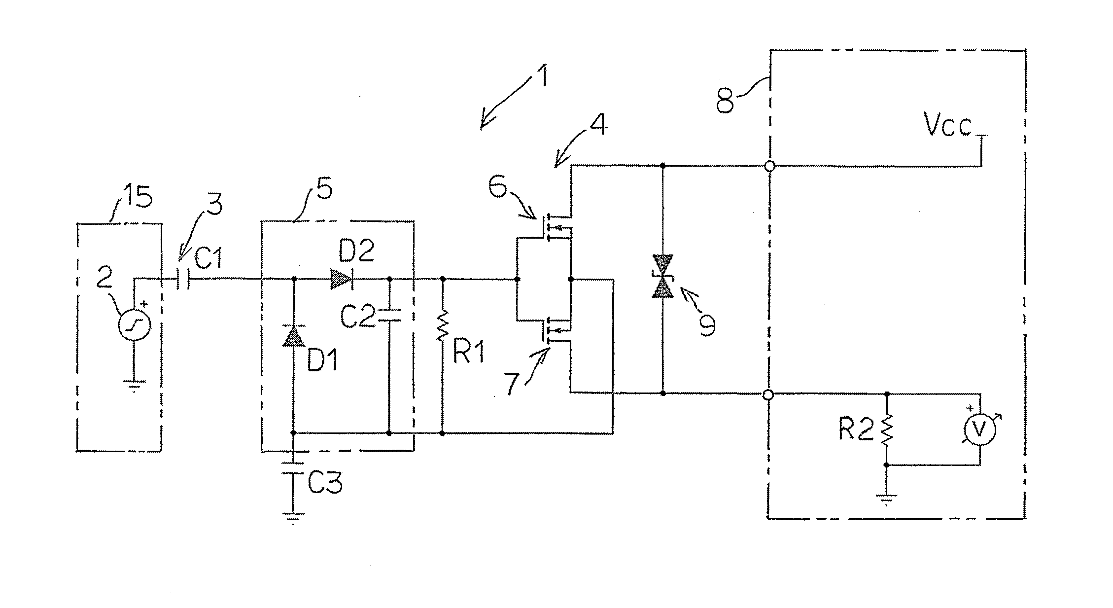
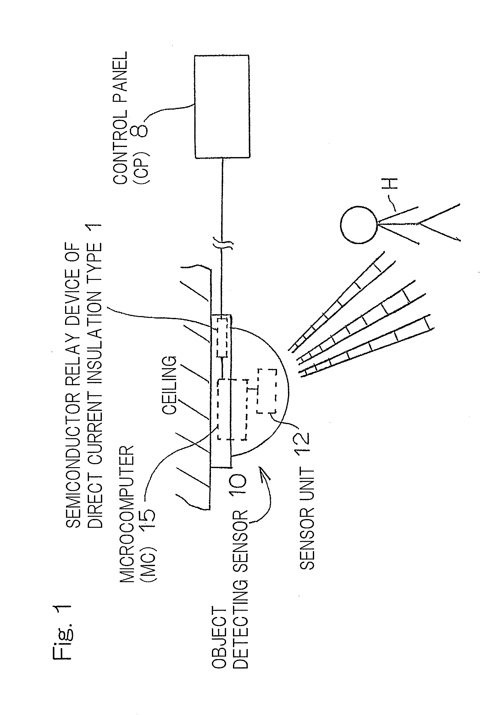
[0025]Hereinafter a preferred embodiment of the present invention will be described in detail with reference to the accompanying drawings. Of those drawings, FIG. 1 illustrates a side view of an object detecting sensor 10, which is a switching equipment having a semiconductor relay device 1 of a direct current insulation type designed in accordance with a preferred embodiment of the present invention is built therein. A control panel (CP) 8 is not only a relay output side machinery for receiving a relay output from the object detecting sensor 10, but also supplies an electric power to the object detecting sensor 10. In the embodiment now under discussion, the control panel (CP) 8 is of a GND common type in which in a connected condition with the electric power supplied to the semiconductor relay device 1, GND (ground) is common.

[0026]The object detecting sensor 10 referred to above is in the form of, for example, a passive type infrared (PIR) sensor affixed to, for example, a ceilin...


PUM


Abstract

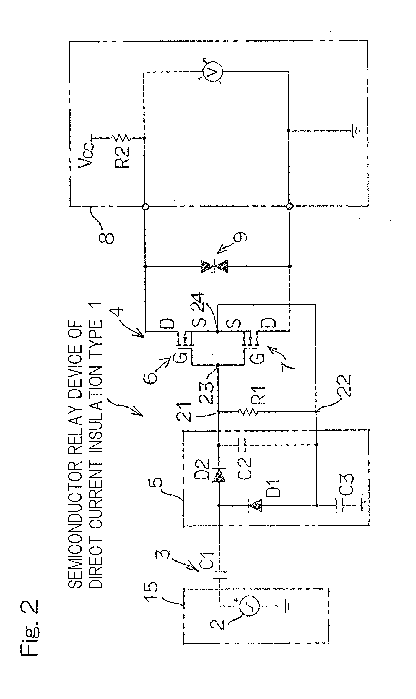
A semiconductor relay device (1) includes a signal input unit (2) for inputting an alternating current signal for relay driving purpose, a direct current insulation member (3) for blocking a direct current electricity of the alternating current signal, a voltage multiplying circuit (5) for multiplying the signal voltage, after the direct current electricity has been blocked, by an integer number, and a relay circuit (4) including two metal-oxide semiconductor field-effect transistors (6, 7) having respective sources connected with each other and connected in a reverse series with each other and also having respective gates connected with each other. Those metal-oxide semiconductor field-effect transistors (6, 7) are caused to undergo a bidirectional ON-Off operation when the respective gates of those metal-oxide semiconductor field-effect transistors (6, 7) are brought into a conducting state by a signal of which voltage has been multiplied by the voltage multiplying circuit (5).

Description

CROSS REFERENCE TO THE RELATED APPLICATION[0001]This application is based on and claims Convention priority to Japanese patent application No. 2011-126228, filed Jun. 6, 2011, the entire disclosure of which is herein incorporated by reference as a part of this application.BACKGROUND OF THE INVENTION[0002]1. Field of the Invention[0003]The present invention relates to a semiconductor relay device of a direct current insulation type having two metal-oxide semiconductor field-effect transistors (MOSFETs) that are connected in series with each other.[0004]2. Description of Related Art[0005]In this type of insulation type semiconductor relay device, a metal oxide semiconductor (MOS) relay has been known which undergoes an ON-OFF operation by conducting a gate of a MOSFET upon impingement of rays of light, emitted from a light emitting diode (LED), upon a photo diode array. In this respect, see, for example, the patent document 1 listed below. The photo MOS relay referred to above is of a...

Claims


Application Information

Patent Timeline
IPC IPC(8): H03K17/94
CPCH03K17/941G01J1/46G01J5/34G08B13/19H03K17/6874H03K17/689
Inventor MURATA, YASUHITO
Owner OPTEX CO LTD
Learn More