
Graphene nanoribbon sensor

a graphene nanoribbon and sensor technology, applied in the field of sensors, can solve the problems of low conductivity of graphene oxide, low sensing sensitivity, and small defects of graphene, and achieve the effect of high sensing sensitivity

Inactive Publication Date: 2014-04-17
ELECTRONICS & TELECOMM RES INST
View PDF2 Cites 20 Cited by
  • Summary
  • Abstract
  • Description
  • Claims
  • Application Information

AI Technical Summary

Benefits of technology

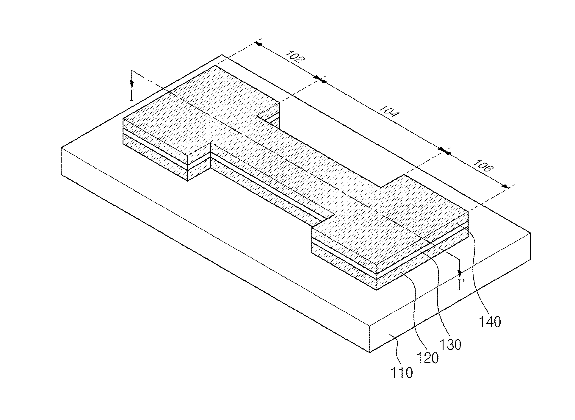
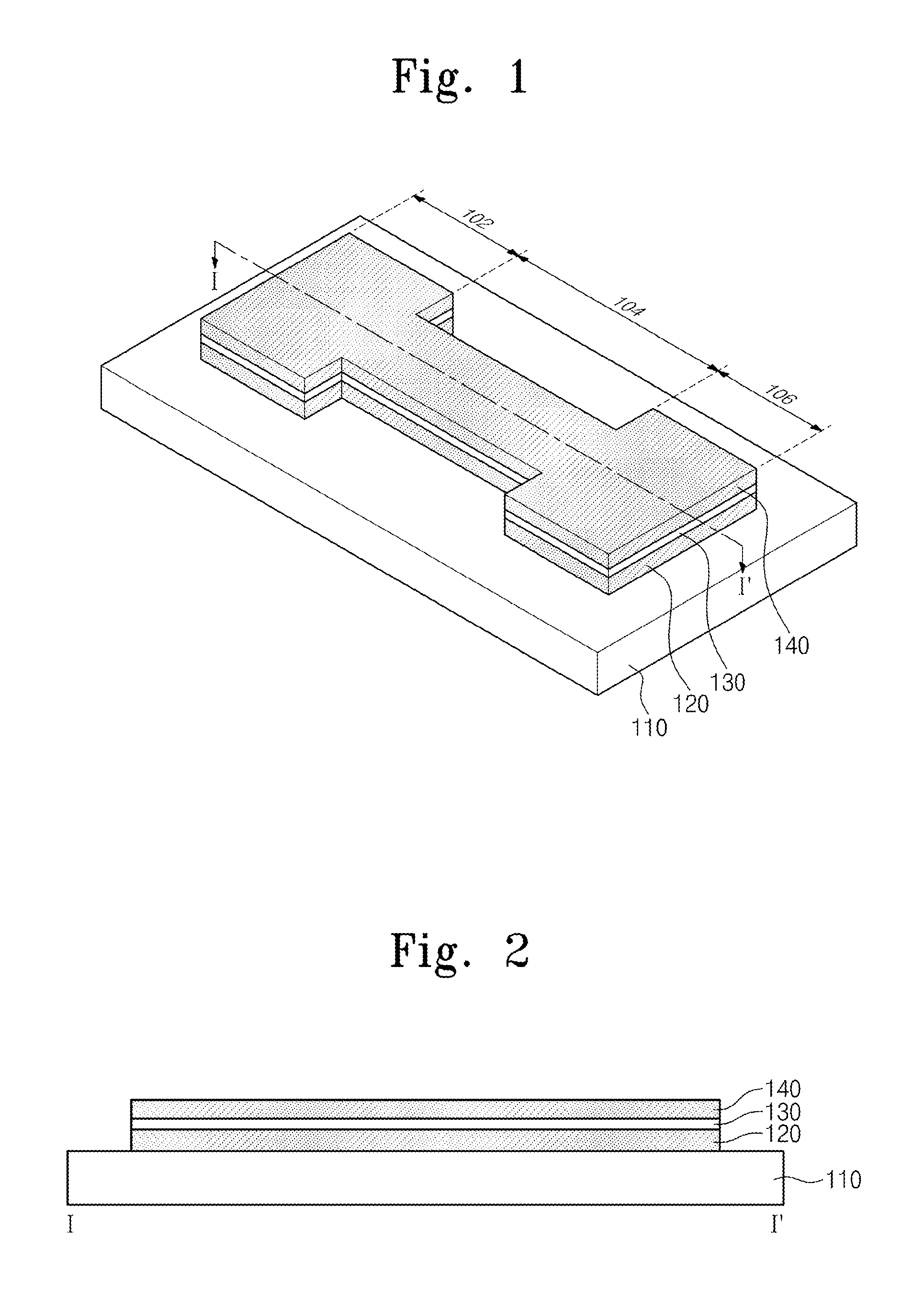
This patent describes a new type of sensor made from a layer of graphene called a nanoribbon. The sensor is very sensitive and can detect small changes in the chemical structure of the graphene layer. This makes it ideal for use in various applications where the detection of small molecules or ions is important. The sensor has a layer of graphene on a substrate, with a smaller channel region in between the larger electrode regions. The edge of the graphene layer is exposed from the dielectric layer, and the channel region is only about 100 nanometers wide. The sensor may include a lower dielectric layer between the substrate and the graphene layer, which may be made of hexagonal boron nitride. The lower dielectric layer, graphene layer, and upper dielectric layer may all have the same width or a ribbon shape in the first direction. The technical effect of this new sensor is its high sensitivity and ability to detect small changes in chemical structure of the graphene layer.

Problems solved by technology

Basically, however, graphene has a high conductivity but small defects, and is thus unlikely to be used to measure molecules.
Also, a graphene oxide has a low conductivity due to a number of defects.
However, application of graphene to a sensor is now limited in a state where graphene losses its high electron transporting ability due to such defects.

Method used


Image

  • Graphene nanoribbon sensor
  • Graphene nanoribbon sensor

Examples


Embodiment Construction

[0017]Hereinafter, preferred embodiments of the inventive concept will be described in detail with reference to the accompanying drawings in such a manner that the technical idea of the inventive concept may easily be carried out by a person with ordinary skill in the art to which the invention pertains. The present disclosure may, however, be embodied in different forms and should not be construed as limited to the embodiments set forth herein.

[0018]In the drawings, anything unnecessary for describing the present disclosure will be omitted for clarity, and also like reference numerals in the drawings denote like elements.

[0019]In the specification and in all the claims, when it is described that one comprises (or includes or has) some elements, it should be understood that it may comprise (or include or has) only those elements, or it may comprise (or include or have) other elements as well as those elements if there is no specific limitation.

[0020]It will be understood that when a...


PUM

PropertyMeasurementUnit
widthaaaaaaaaaa
widthaaaaaaaaaa
dielectricaaaaaaaaaa

Abstract

Provided is a graphene nanoribbon sensor. The sensor includes a substrate, a graphene layer formed on the substrate in a first direction, and an upper dielectric layer on the graphene layer. Here, the graphene layer may have a plurality of electrode regions respectively separated in the first direction and a channel between the plurality of electrode regions.

Description

CROSS-REFERENCE TO RELATED APPLICATIONS[0001]This U.S. non-provisional patent application claims priority under 35 U.S.C. §119 of Korean Patent Application No. 10-2012-0115434, filed on Oct. 17, 2012, the entire contents of which are hereby incorporated by reference.BACKGROUND OF THE INVENTION[0002]The inventive concept disclosed herein relates to a sensor, and more particularly, to a graphene nanoribbon sensor.[0003]Recently, research and development have been actively conducted on a sensor using materials having a superior conductivity such as graphene or graphene oxide (GO). Graphene is applicable to a sensor sensing molecules within a gas and bio materials by measuring surface defects and a decrease in conductivity resulted from a change of an sp2-bonded structure into an sp3-bonded structure due to the bonding between molecules to be measured. Basically, however, graphene has a high conductivity but small defects, and is thus unlikely to be used to measure molecules. Also, a gr...

Claims


Application Information

Patent Timeline
Patent Type & Authority Applications(United States)
IPC IPC(8): G01N27/414
CPCB82Y15/00G01N27/414B82Y40/00G01N27/127G01N27/30
Inventor YU, YOUNG-JUNCHOI, CHOON GI
Owner ELECTRONICS & TELECOMM RES INST
Learn More