

Semiconductor device
a technology of semiconductors and transistors, applied in the direction of semiconductor devices, basic electric elements, electrical equipment, etc., can solve the problems of electrical characteristics deformation and electrical characteristics of transistors to deteriorate, and achieve the effect of favorable electrical characteristics and high reliability
- Summary
- Abstract
- Description
- Claims
- Application Information
AI Technical Summary
Benefits of technology
Problems solved by technology
Method used
Image

Examples
embodiment 1
[0053]In this embodiment, a stacked-layer structure of a semiconductor device of one embodiment of the present invention will be described with reference to FIG. 10.
Stacked-Layer Structure
[0054]FIG. 10 is a conceptual view of an example of the stacked-layer structure.
[0055]The stacked-layer structure of the semiconductor device includes an oxide stack 404 between a base insulating layer 402 and a gate insulating layer 410. Further, the oxide stack 404 includes a first oxide layer 404a, an oxide semiconductor layer 404b, and a second oxide layer 404c.
[0056]Each of the first oxide layer 404a and the second oxide layer 404c is an oxide layer containing one or more kinds of metal elements which form the oxide semiconductor layer 404b.
[0057]The oxide semiconductor layer 404b includes a layer represented by an In-M-Zn oxide, which contains at least indium, zinc, and M (M is a metal element such as Al, Ga, Ge, Y, Zr, Sn, La, Ce, or Hf). The oxide semiconductor layer 404b preferably conta...
embodiment 2
[0132]In this embodiment, one embodiment of a semiconductor device including the stacked structure described in Embodiment 1 will be described with reference to FIGS. 1A to 1D, FIGS. 2A to 2C, FIGS. 3A to 3D, FIGS. 9A to 9C, and FIG. 19. In this embodiment, a top gate transistor including an oxide semiconductor layer will be described as an example of the semiconductor device.
Structural Example 1 of Semiconductor Device
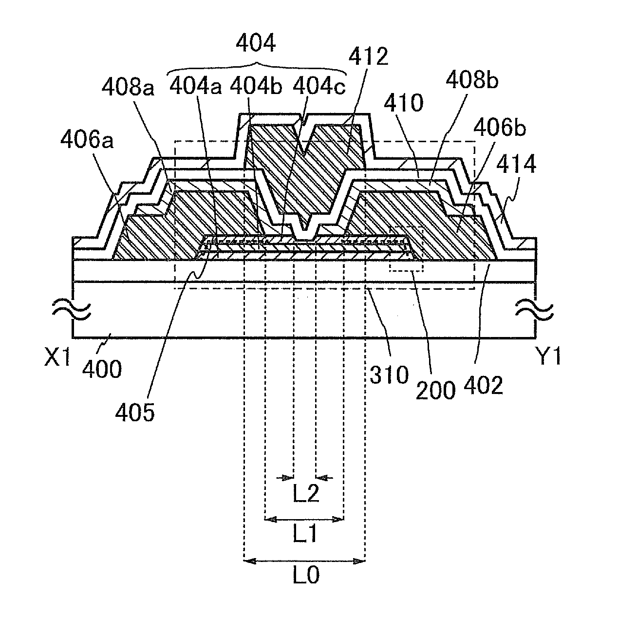
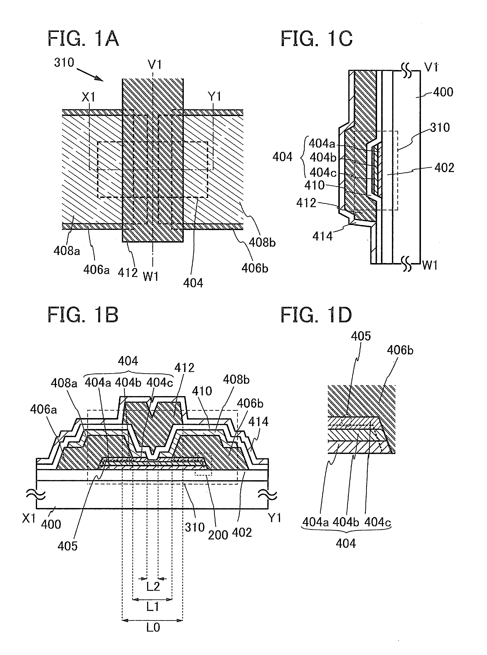
[0133]FIGS. 1A to 1D illustrate a structural example of a transistor 310. FIG. 1A is a plan view of the transistor 310, FIG. 1B is a cross-sectional view taken along dashed-dotted X1-Y1 in FIG. 1A, and FIG. 1C is a cross-sectional view taken along dashed-dotted V1-W1 in FIG. 1A. FIG. 1D is a partial enlarged view of a region 200 in FIG. 1B. Note that in FIG. 1A, some components of the transistor 310 (e.g., a protective insulating layer 414 and the like) are not illustrated to avoid complexity.
[0134]The transistor 310 illustrated in FIGS. 1A to 1D includes the base ins...
example 4
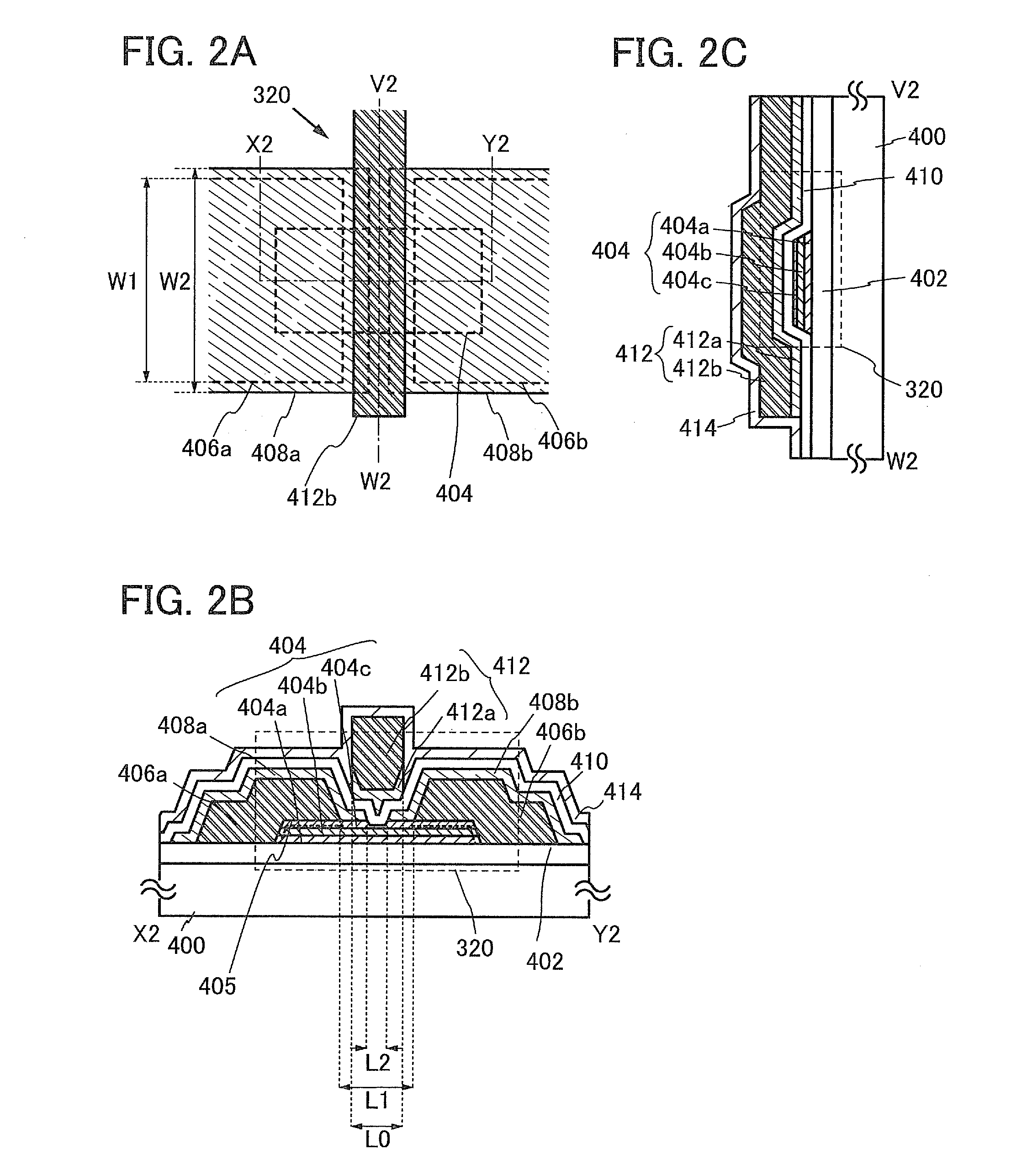
Structural Example 4 of Semiconductor Device
[0181]FIGS. 9A to 9C illustrates a structural example of a transistor 350. The transistor 350 is a modification example of the transistor 320 in FIGS. 2A to 2C. FIG. 9A is a plan view of the transistor 350, FIG. 9B is a cross-sectional view taken along line X3-Y3 in FIG. 9A, and FIG. 9C is a cross-sectional view taken along line V3-W3 in FIG. 9A. Note that in FIG. 9A, some components of the transistor 350 (e.g., the protective insulating layer 414 and the like) are not illustrated to avoid complexity.
[0182]A difference between the transistor 320 and the transistor 350 is a stacking order of the oxide stack 404 and the source electrode layer and the drain electrode layer. That is, in the transistor 350, the first source electrode layer 406a and the first drain electrode layer 406b are provided so as to cover side faces of an island-shaped first oxide layer 407a in a channel length direction, and side faces in the channel length direction an...
PUM
 Abstract
Description
Claims
Application Information