Fingerprint sensor and button combinations and methods of making same
What is Al technical title?
Al technical title is built by PatSnap Al team. It summarizes the technical point description of the patent document.
a technology which is applied in the field of fingerprint sensor and button combination and methods of making same, can solve the problems of often impractical system use of components
Active Publication Date: 2014-04-17
SYNAPTICS INC
View PDF3 Cites 92 Cited by
Summary
Abstract
Description
Claims
Application Information
AI Technical Summary
This helps you quickly interpret patents by identifying the three key elements:
Problems solved by technology
Method used
Benefits of technology
[0010]A user interface, e.g., a button, suitable for incorporation into an electronic device, such as a laptop, tablet, or smart phone or other portable computing devices is disclosed, as well as methods of use and methods of manufacture. The interface can have a housing with a small profile with a thickness less than or equal to 3 mm, an upper layer which fits within a user device housing and sits atop one or more sets of sensor traces in communication with a chip external to the interface via a flexible circuit.
[0011]An aspect of the disclosure is directed to an electronic device user interface. Suitable electronic device user interfaces can comprise: a housing having side walls defining an open upper end and a lower surface; a biometric sensor capable of sensing a target biometric parameter having a sensor interface with a sensing side wherein the sensor interface is capable of positioning within the open upper end of the housing; a protective coating on the sensing side of the sensor interface; and an integrated circuit, external to the housing, in communication with the biometric sensor. In some aspects, the protective coating extends over or through one or more side walls of the housing.
[0012]Additionally, the biometric sensor further can comprise a flexible circuit substrate and at least one conductive trace connecting the biometric sensor to the integrated circuit. The conductive traces of the flexible circuit substrate can also be positionable on at least one of a side of the flexible circuit substrate facing towards an exterior of the housing and a side of the flexible circuit substrate facing towards an interior of the housing. In some configurations, the device can further comprise one or more of each of: a potting material positionable between the lower surface of the housing and the protective coating; a bezel extending from the side walls of the housing above the bottom of the protective covering; and a removable bottom plate that can attach to the housing to support the biometric sensor. In some configurations, the flexible circuit can wrap around the removable bottom plate. Additionally, an adhesive potting material can be provided between the bottom plate and the protective coating. In still other aspects, the biometric sensor can be capable of capturing a fingerprint from a finger of a user.
[0013]Additional aspects of the disclosure are directed to a method of fabricating an electronic device user interface. The method can comprise: providing a biometric sensor having a sensor interface with a sensing side and one or more conductive traces thereon in communication with a flexible circuit; placing a protective coating on the sensing side of the biometric sensor; inserting the biometric sensor into a housing; and providing an integrated circuit external to the housing in communication with the biometric sensor. An additional step can include: forming the protective coating over one or more side walls of the housing. The biometric sensor can be comprised of a flexible circuit having a flexible substrate, wherein the method further comprises the step of: forming at least one conductive trace connecting the biometric sensor to the integrated circuit.
[0014]Yet another step can include forming the one or more conductive traces of the flexible circuit on at least one of a side of the flexible substrate adjacent a finger of a user and a side of the flexible substrate facing away from the finger. Still other steps can include one or more of each of: providing an adhesive between the bottom portion of the housing and the protective coating; forming a bezel over at least the edges of the protective covering; providing a bottom plate that attaches to the housing to enclose the biometric sensor; forming the flexible circuit around the bottom plate; and providing an adhesive between the bottom plate and the protective coating.
Problems solved by technology
However, the widespread adoption of fingerprint sensing technology in a broad range of applications has faced a number of obstacles.
Additionally, such components are often impractical for use in systems that are designed to be of minimal size or weight.
Method used
Image
Click on the blue label to locate the original text in one second.
Reading with bidirectional positioning of images and text.
Examples
Embodiment Construction
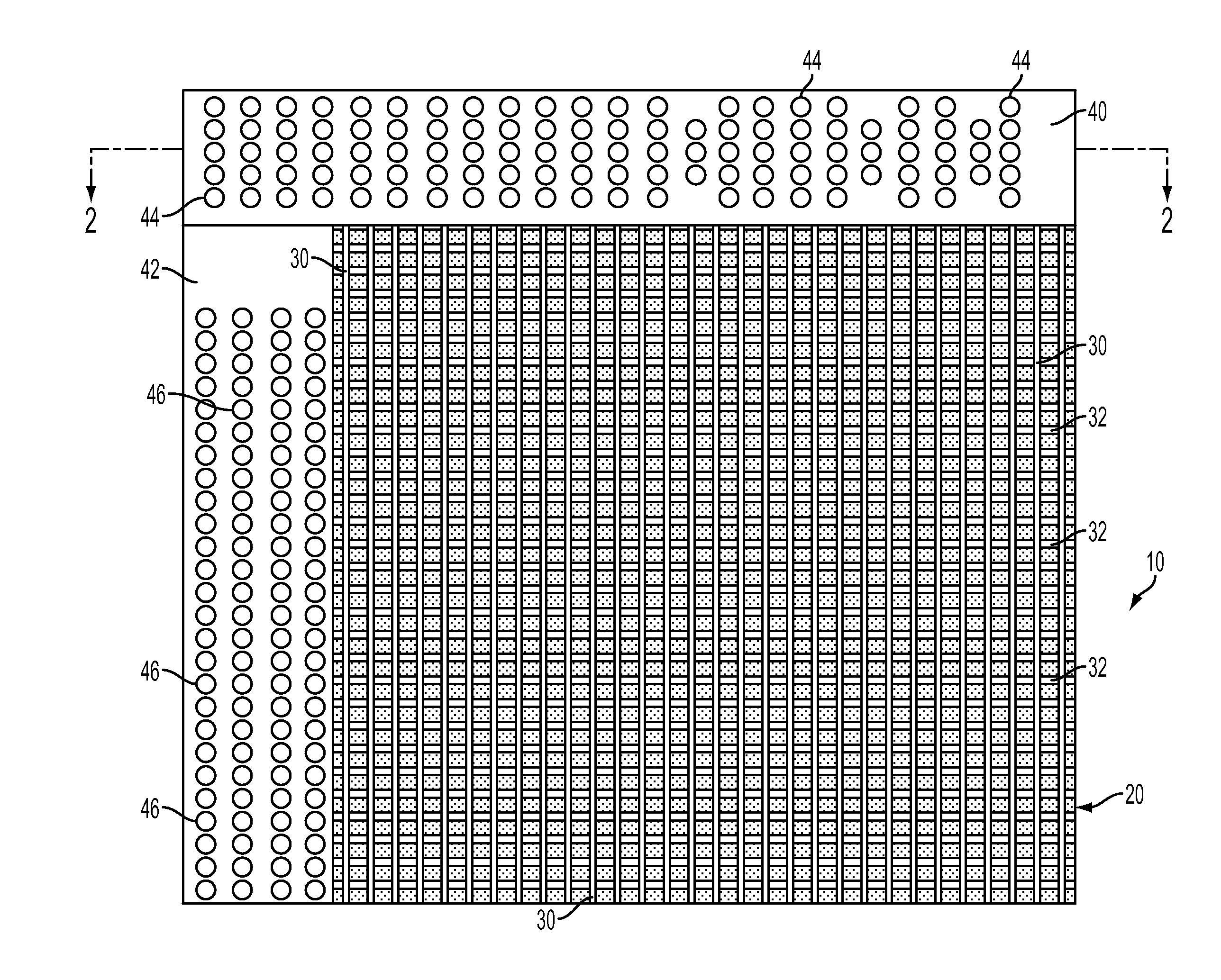
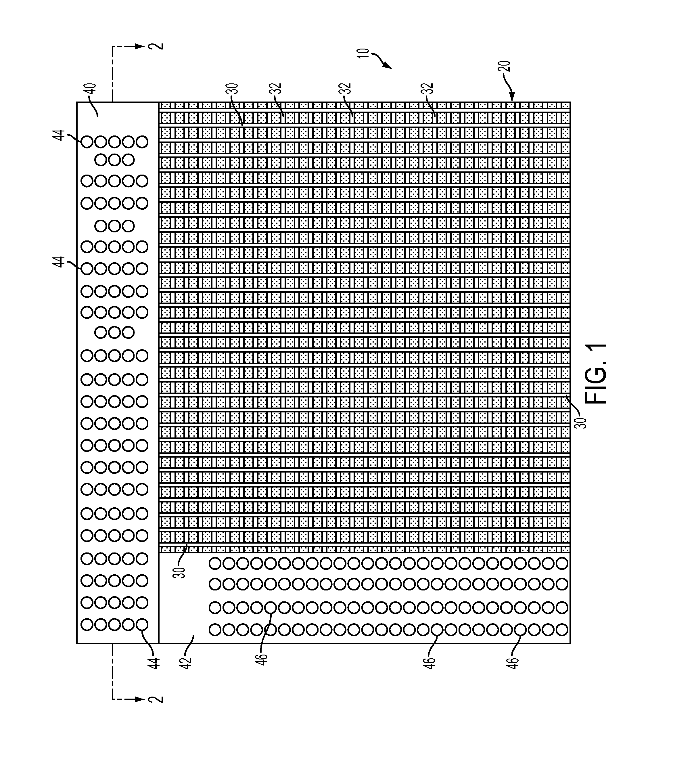
[0032]According to aspects of embodiments of the disclosed subject matter a sensor support housing / package 10, as illustrated schematically in FIG. 1, is disclosed. The sensor 10 may be a biometric sensor, e.g., a fingerprint sensor having a plurality of pixel locations formed in either a linear one dimensional (“1D”) array or a two dimensional grid (“2D”) array, such as is shown schematically in FIG. 1. As shown by way of example in FIG. 1, the 2D sensor array 10 may form a grid 20, having transmit / drive signal vertical traces 30 and generally perpendicular horizontal receiver signal traces 32. The sensor 10 can also be seen to include a transmit / drive signal via section 40 to the top of the schematic illustration in FIG. 1, including transmit / drive signal vias 44 and a receiver signal via section 42 to the left side of the illustration in FIG. 1, including receiver / response signal vias 46. It will be understood by those skilled in the art that the schematic view of FIG. 1 is not t...
PUM
Property
Measurement
Unit
thickness
aaaaa
aaaaa
width
aaaaa
aaaaa
width
aaaaa
aaaaa
Abstract
It will be understood by those skilled in the art that there is disclosed in the present application a biometric sensor that may comprise a plurality of a first type of signal traces formed on a first surface of a first layer of a multi-layer laminate package; at least one trace of a second type, formed on a second surface of the first layer or on a first surface of a second layer of the multi-layer laminate package; and connection vias in at least the first layer electrically connecting the signal traces of the first type or the signal traces of the second type to respective circuitry of the respective first or second type contained in an integrated circuit physically and electrically connected to one of the first layer, the second layer or a third layer of the multilayer laminate package.
Description
CROSS-REFERENCE[0001]This application claims priority to U.S. Provisional Patent Application Ser. Nos. 61 / 713,550, filed on Oct. 14, 2012, entitled FINGERPRINT SENSOR HAVING FLIP CHIP PACKAGING and 61 / 754,287, filed on Jan. 18, 2013, entitled COMPACT BUTTON CONFIGURATIONS AND METHODS, the contents of which are incorporated herein.BACKGROUND OF THE INVENTION[0002]Biometric sensors and imagers, including, e.g., fingerprint sensors and imagers like those disclosed in the present application are known in the art and are disclosed, e.g., in U.S. Pat. No. 7,099,496 to Benkley, issued Aug. 29, 2006, for SWIPED APERTURE CAPACITIVE FINGERPRINT SENSING SYSTEMS AND METHODS; U.S. Pat. No. 7,463,756 to Benkley, issued Dec. 9, 2009, for FINGER POSITION SENSING METHODS AND APPARATUS; to Benkley, issued Apr. 24, 2012, for METHOD AND APPARATUS FOR FINGERPRINT MOTION TRACKING USING AN IN-LINE ARRAY FOR USE IN NAVIGATION APPLICATIONS; U.S. Pat. No. 7,751,601 to Benkley, issued Jul. 6, 2010, for FINGER...
Claims
Application Information
Patent Timeline
Application Date:The date an application was filed.
Publication Date:The date a patent or application was officially published.
First Publication Date:The earliest publication date of a patent with the same application number.
Issue Date:Publication date of the patent grant document.
PCT Entry Date:The Entry date of PCT National Phase.
Estimated Expiry Date:The statutory expiry date of a patent right according to the Patent Law, and it is the longest term of protection that the patent right can achieve without the termination of the patent right due to other reasons(Term extension factor has been taken into account ).
Invalid Date:Actual expiry date is based on effective date or publication date of legal transaction data of invalid patent.
Patent Type & Authority Applications(United States)