Methods for modeling interactions between massively coupled multiple vias in multilayered electronic packaging structures

a multi-layered electronic packaging and interaction technology, applied in the field of numerical simulation of reflected, transmitted, coupled signals in respect of multi-layered structures, can solve the problems of high densities, considerable design problems, and fast simulation of packages, and achieve rapid and accurate simulation of coupling effects, easy integration into a system simulation, and accurate results.

Active Publication Date: 2006-12-12
UNIV OF WASHINGTON
View PDF8 Cites 47 Cited by
  • Summary
  • Abstract
  • Description
  • Claims
  • Application Information

AI Technical Summary

Benefits of technology

[0017]Multilayered structures can be simulated by using the technique of transfer matrix. The numerical model is then further developed to account for more complicated structures that contain from two to hundreds (or thousands of vias). The present invention preferably uses the Foldy-Lax equations for solving the multiscattering problem. This set of equations relates the incident wave to the exciting wave from the source and to all the scattered waves from other cylinders, thus accurately accounting for interactions among all of the vias. The simulation paradigm developed in the present invention yields accurate results that are essentially independent of either the number of vias involved or the effective radii of via pins in the package. The invention can be used to rapidly and accurately simulate the coupling effects of hundreds of massively-coupled vias in a densely packaged circuit, and in printed circuit boards.
[0018]Th

Problems solved by technology

The construction of physical prototypes and long design cycles are undesirable, and hence, rigorous, accurate, and fast simulation of packages is required.
These packages are used extensively, primarily because of high speed, high densities, and routing complexity.
This lack of localization poses considerable design problems, particularly at high frequencies, in achieving reliability, high speed, and in implementing a simulation.
Such coupling can even cause unreliable behavior or complete signal failure, along with signal integrity loss, longer delays, and inappropriate switching of signals.
If such signals reach terminal ports, the noise can affect input and output devices through spurious switching signals, thereby degrading system performance.
Unfortunately, these models only function well at very low frequencies.
In particular, propagation and high-frequency scattering effects are not modeled accurately with this method.
Therefore, this method is not suitable for modeling high speed electronic package

Method used


Image

  • Methods for modeling interactions between massively coupled multiple vias in multilayered electronic packaging structures
  • Methods for modeling interactions between massively coupled multiple vias in multilayered electronic packaging structures
  • Methods for modeling interactions between massively coupled multiple vias in multilayered electronic packaging structures

Examples


Embodiment Construction

Overview of the Present Invention

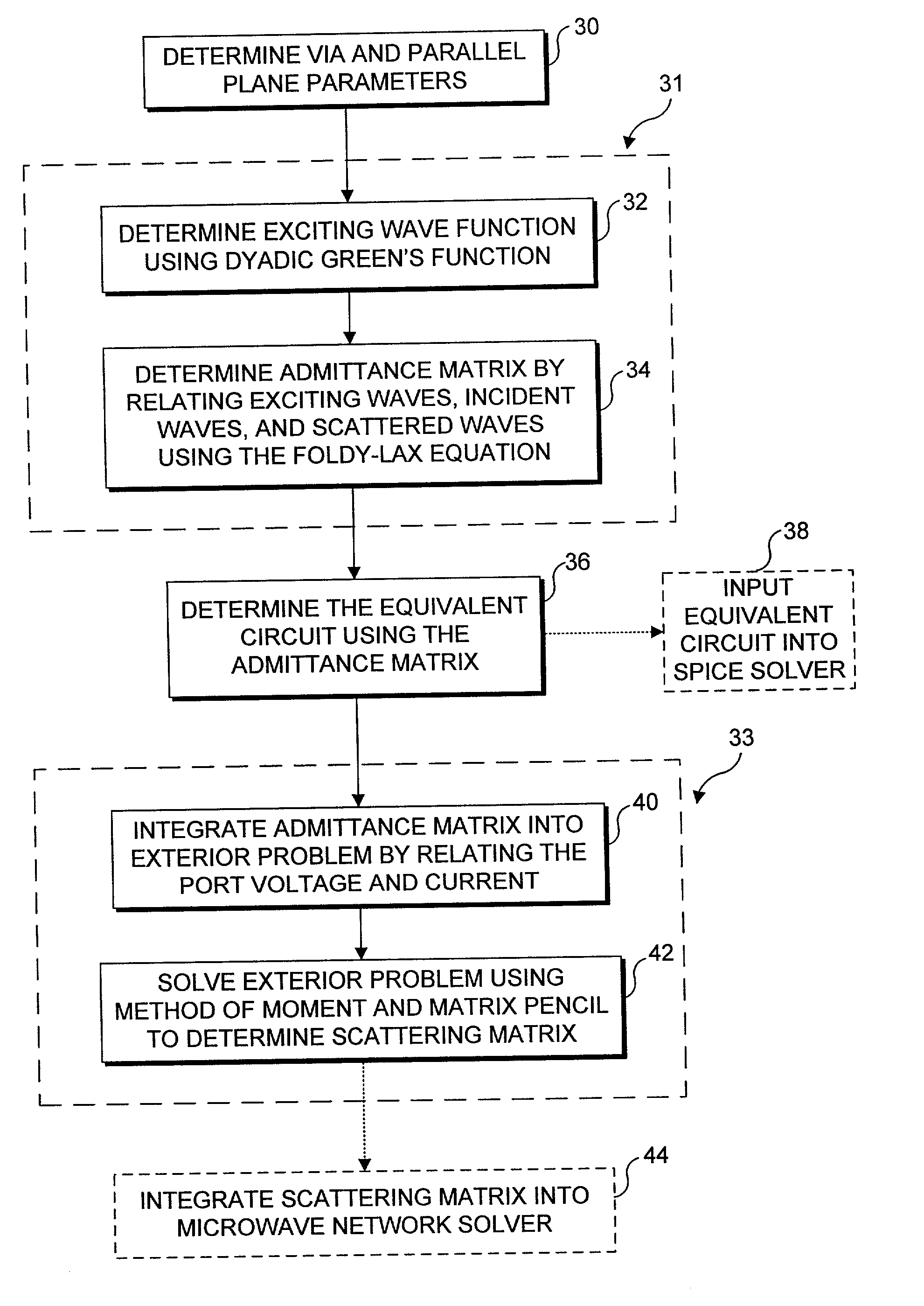
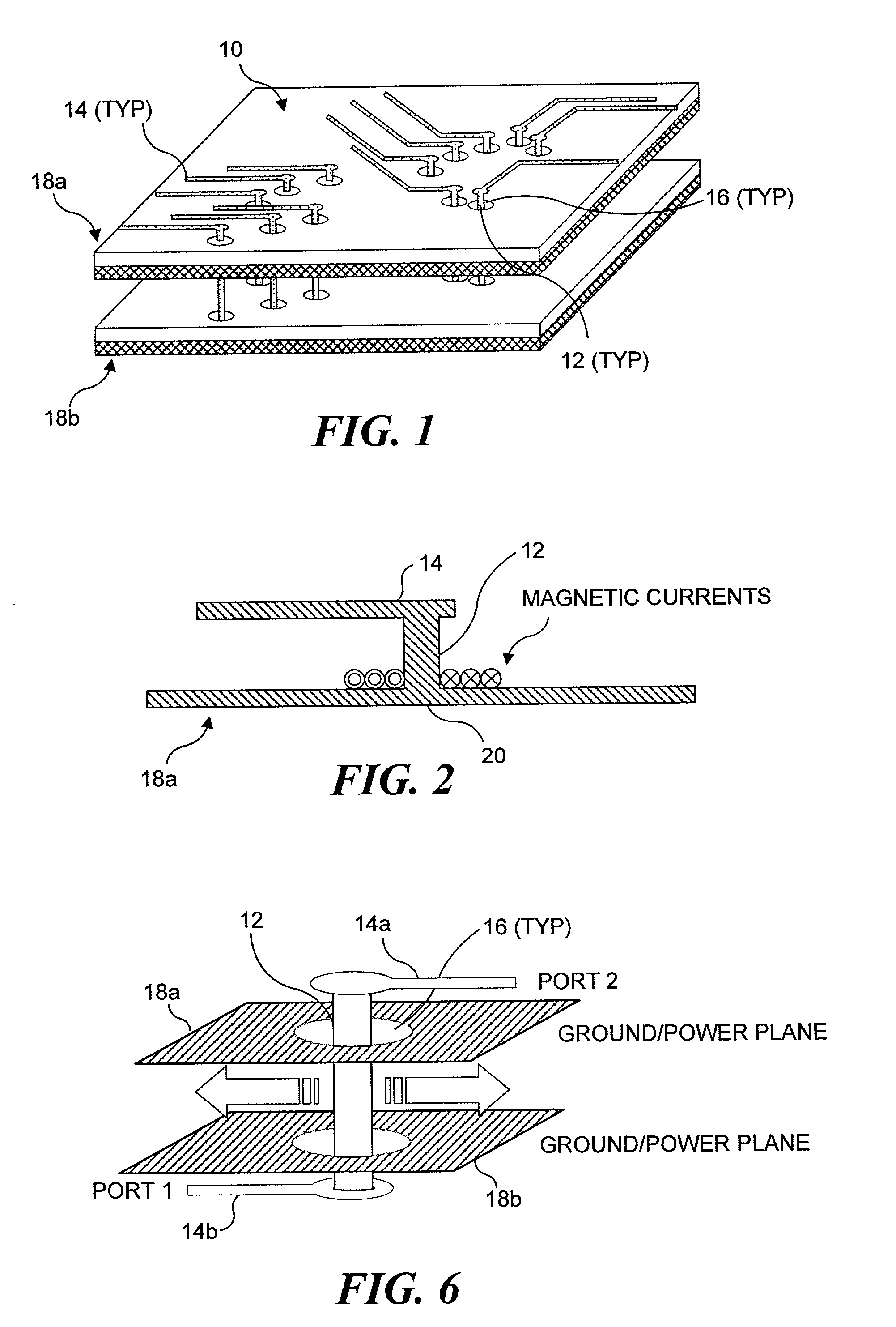
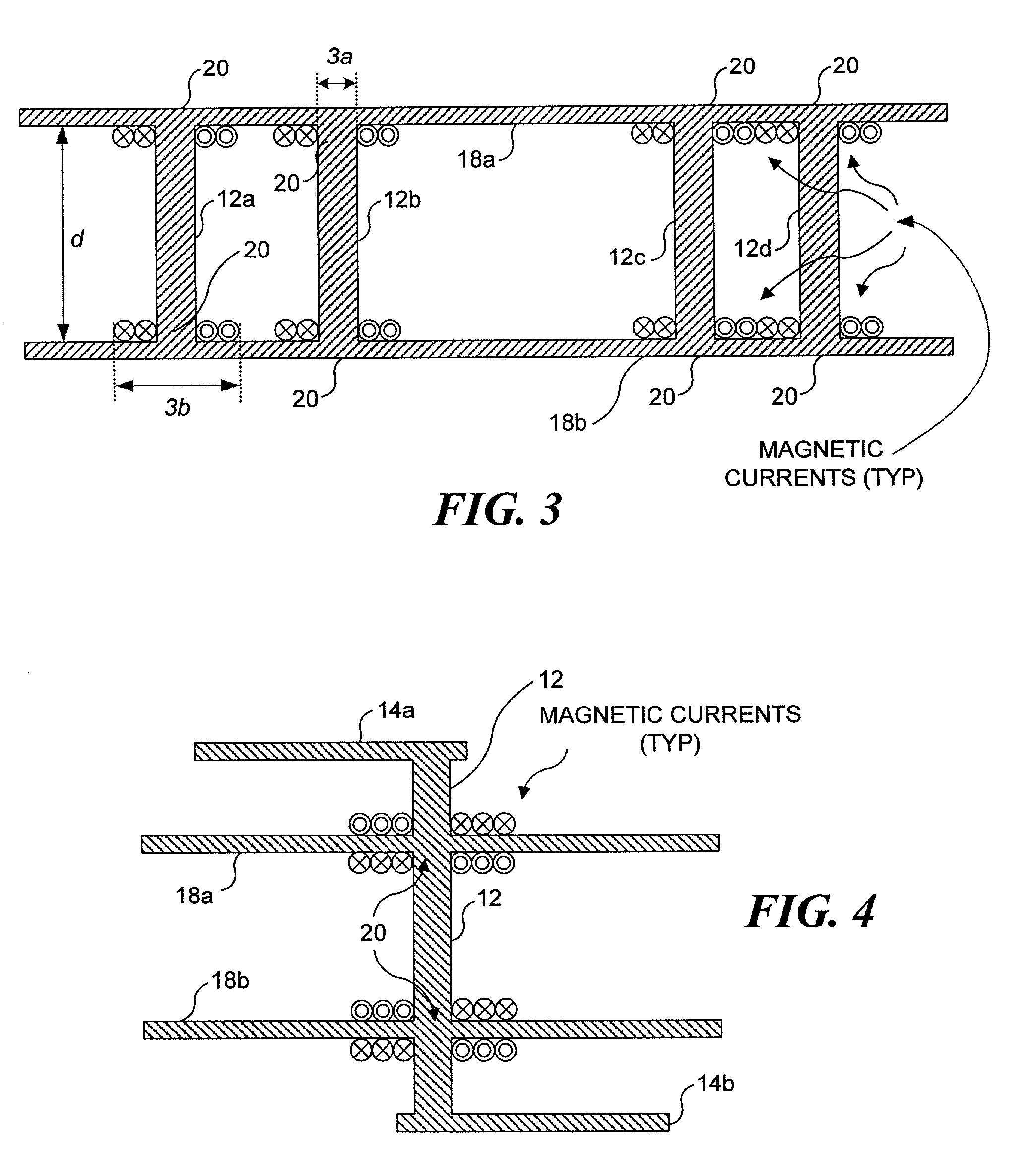
[0042]FIG. 1 schematically illustrates a multilayered electronic package 10 with multiple parallel, or nearly parallel, conducting ground and power planes that are separated by dielectric substrates. A plurality of via structures 12 are clearly shown connecting together traces 14 residing in / on different layers or planes. Each via passes through a corresponding aperture 16. The layered geometry includes matched ground and power planes 18a and 18b, defined by metallic layers separated by dielectric layers.

[0043]Consider the problem of modeling the dynamics of traces 14 connected to vias 12. Each via 12 passes through a corresponding aperture 16 in ground / power planes 18a and 18b of FIG. 1. For each matched pair of ground / power planes, the paired planes will form a parallel-plate waveguide (i.e., ground / power plane 18a forms a first parallel-plate waveguide, and ground / power plane 18b forms a second parallel-plate waveguide). By using the equivalence p...


PUM


Abstract

Analyzing interactions between vias in multilayered electronic packages that include at least two spaced-apart conducting planes, and multiple vias that connect signal traces on different layers. Voltages at active via ports are represented as magnetic ring current sources, which generate electromagnetic modes inside the plane structure. Substantial electromagnetic coupling between vias occurs. A full-wave solution of multiple scattering among cylindrical vias in planar waveguides is derived using Foldy-Lax equations. By using the equivalence principle, the coupling is decomposed into interior and exterior problems. For the interior problem, the dyadic Green's function is expressed in terms of vector cylindrical waves and waveguide modes. The Foldy-Lax equations for multiple scattering among the cylindrical vias are applied, and waveguide modes are decoupled in the Foldy-Lax equations. The scattering matrix of coupling among vias is then calculated for use in determining signal reflection, transmission, and/or coupling in the electronics package.

Description

RELATED APPLICATIONS[0001]This application is based on a prior copending provisional application Ser. No. 60 / 294,657, filed on May 30, 2001, the benefit of the filing date of which is hereby claimed under 35 U.S.C. §119(e).FIELD OF THE INVENTION[0002]This invention generally pertains to the numerical simulation of reflected, transmitted, and coupled signals in respect to vias in structures having multilayered geometry, and more specifically, to an adaptation of the Foldy-Lax multiple scattering formula for modeling signal distortion and coupling between massively coupled multiple vias in multilayered chip packages, chip substrates, and printed circuit boards.BACKGROUND OF THE INVENTION[0003]Components and devices utilizing electrical circuits involving integrated circuit (IC) chips, multi-chip modules, printed circuit boards, connectors, back planes, and cards are generally referred to as electronic packaging. The terms “electronic packaging structure,”“electronic package,” and “pac...

Claims


Application Information

Patent Timeline
IPC IPC(8): G06F17/10G06F17/50H05K7/00
CPCG06F17/5036G06F30/367
Inventor TSANG, LEUNGCHEN, HOUFEIHUANG, CHUNGCHIJANDHYALA, VIKRAM
Owner UNIV OF WASHINGTON
Why Eureka
Try Eureka