Chip on film and display device including the same

a display device and film technology, applied in the direction of electrical apparatus construction details, instruments, semiconductor/solid-state device details, etc., can solve the problems of electromagnetic interference and difficult to remove noise, and achieve the effects of reducing electromagnetic interference, reducing electromagnetic interference, and reducing electromagnetic interferen

Inactive Publication Date: 2014-05-01
SAMSUNG DISPLAY CO LTD
View PDF15 Cites 47 Cited by
  • Summary
  • Abstract
  • Description
  • Claims
  • Application Information

AI Technical Summary

Benefits of technology

[0028]In a chip on film according to the exemplary embodiments, it is possible to minimize electromagnetic interference (EMI) in a display device to which the chip on film is connected by forming an electromagnetic wave blocking layer under a driving film by a metal-plated layer to block an electromagnetic wave occurring in a wire la...

Problems solved by technology

Further, since the wire layer of the COF applied to the flexible display device of the thin film is formed of a single layer in order to form a thin chip on film, it is di...

Method used


Image

  • Chip on film and display device including the same
  • Chip on film and display device including the same
  • Chip on film and display device including the same

Examples


Embodiment Construction

[0036]The present invention will be described more fully hereinafter with reference to the accompanying drawings, in which exemplary embodiments of the invention are shown. As those skilled in the art would realize, the described embodiments may be modified in various different ways, all without departing from the spirit or scope of the present invention.

[0037]The drawings and description are to be regarded as illustrative in nature and not restrictive. Like reference numerals designate like elements throughout the specification. The size and thickness of each configuration shown in the drawings are arbitrarily shown for understanding and ease of description, but the present invention is not limited thereto.

[0038]Throughout the specification, it will be understood that when an element such as a layer, film, region, or substrate is referred to as being “on” another element, it can be directly on the other element or intervening elements may also be present.

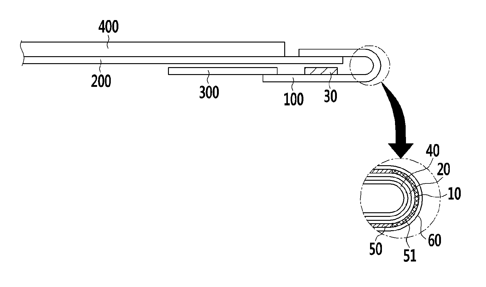
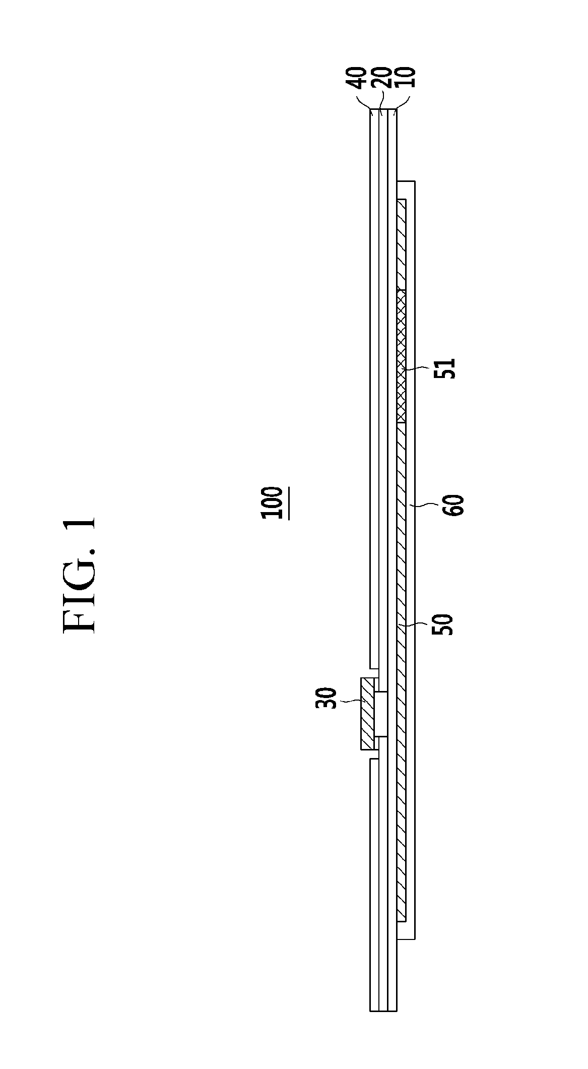
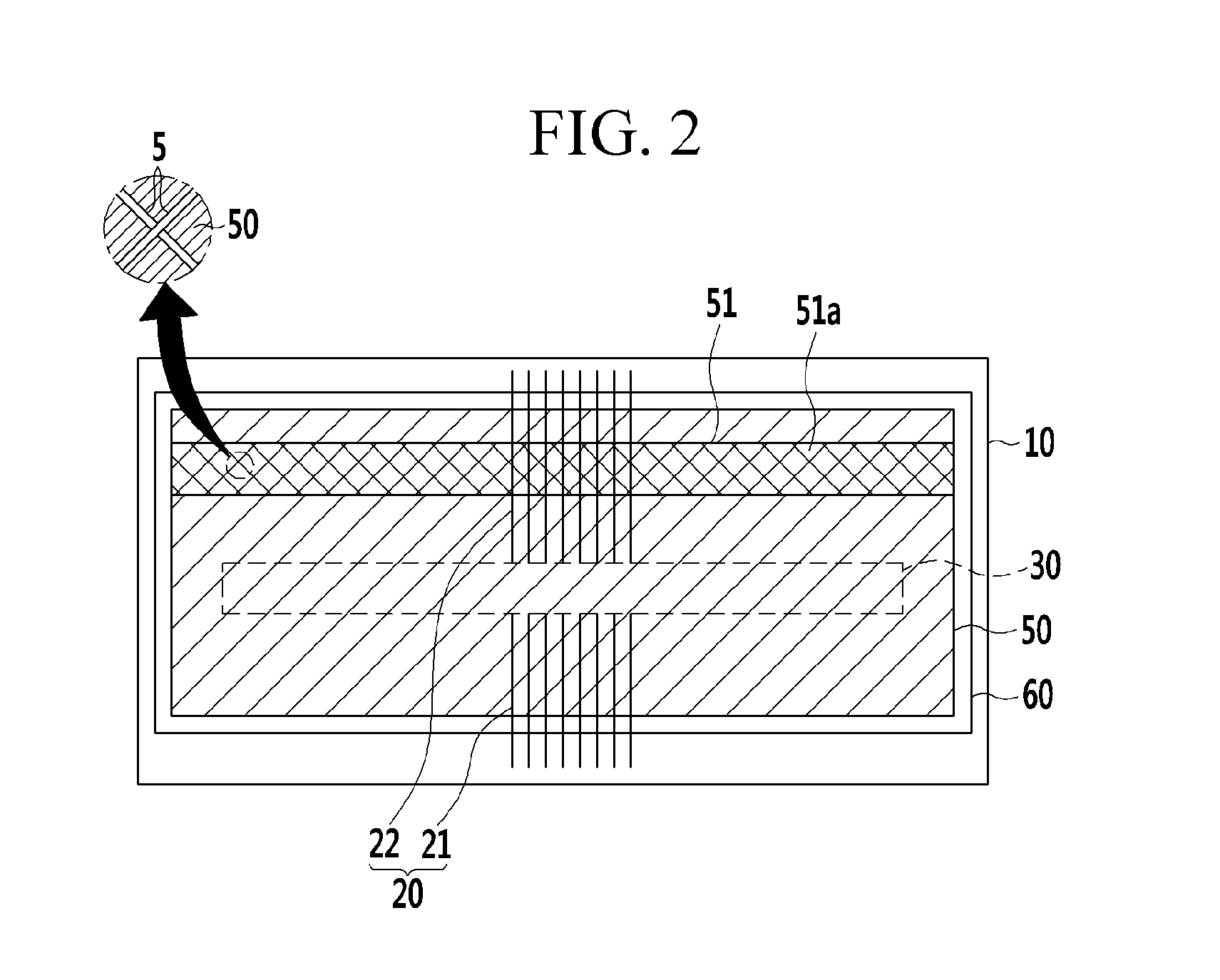
[0039]FIG. 1 is a side view...


PUM


Abstract

A chip on film according to an exemplary embodiment includes: a driving film, a wire layer formed on a first surface of the driving film, a driving chip connected to the wire layer, and an electromagnetic wave blocking layer formed on a second surface of the driving film, in which a mesh portion may be formed on a portion of the electromagnetic wave blocking layer.

Description

CLAIM OF PRIORITY[0001]This application claims priority to and the benefit of Korean Patent Application No. 10-2012-0119149 filed in the Korean Intellectual Property Office on Oct. 25, 2012, the entire contents of which are incorporated herein by reference.BACKGROUND[0002]1. Field[0003]The described technology relates generally to a chip on film and a display device including the same.[0004]2. Description of the Related Art[0005]A display device includes a liquid crystal display (LCD), an organic light emitting diode (OLED) display, and the like, and particularly the OLED display includes a display substrate providing a pixel region and a non-pixel region, and a sealing substrate that is disposed to face the display substrate for encapsulation and attached to the substrate by a sealant such as epoxy. A plurality of light emitting elements connected in a matrix manner between a scan line and a data line to constitute a pixel is formed in the pixel region of the display substrate, and...

Claims


Application Information

Patent Timeline
IPC IPC(8): H05K9/00
CPCG02F1/13452H01L23/4985H01L23/552H01L24/16H05K1/0224H05K9/00H05K1/189H01L2224/16225H05K2201/09681H05K2201/10128H05K1/0281H01L2924/12044H01L2924/12041H01L2924/00H10K59/126
Inventor LEE, HEE-KWON
Owner SAMSUNG DISPLAY CO LTD
Why Eureka
Try Eureka