Touch electrode structure and a method for manufacturing the same

a technology of touch electrodes and manufacturing methods, applied in the field of touch electrodes, can solve the problems of long production time for exposure, development, etching, cleaning steps that are needed during the photolithographic process, and the photolithographic process is very complex, so as to reduce the time spent on removing a large area of the conducting layer, improve production efficiency, and reduce production costs

Active Publication Date: 2014-05-08
TPK TOUCH SOLUTIONS (XIAMEN) INC
View PDF12 Cites 13 Cited by
  • Summary
  • Abstract
  • Description
  • Claims
  • Application Information

AI Technical Summary

Benefits of technology

[0014]Another objective of the present disclosure is to provide a touch panel, a touch electrode structure and a manufacturing method using a laser etching process, which improves production efficiency and reduces production cost. Moreover, in the present disclosure, a plurality of adjacent laser etching lines are generated between the output pins to prevent s

Problems solved by technology

However, the photolithographic process is very complex.
For example, exposure, developing, etching, and clea

Method used


Image

  • Touch electrode structure and a method for manufacturing the same
  • Touch electrode structure and a method for manufacturing the same
  • Touch electrode structure and a method for manufacturing the same

Examples


Embodiment Construction

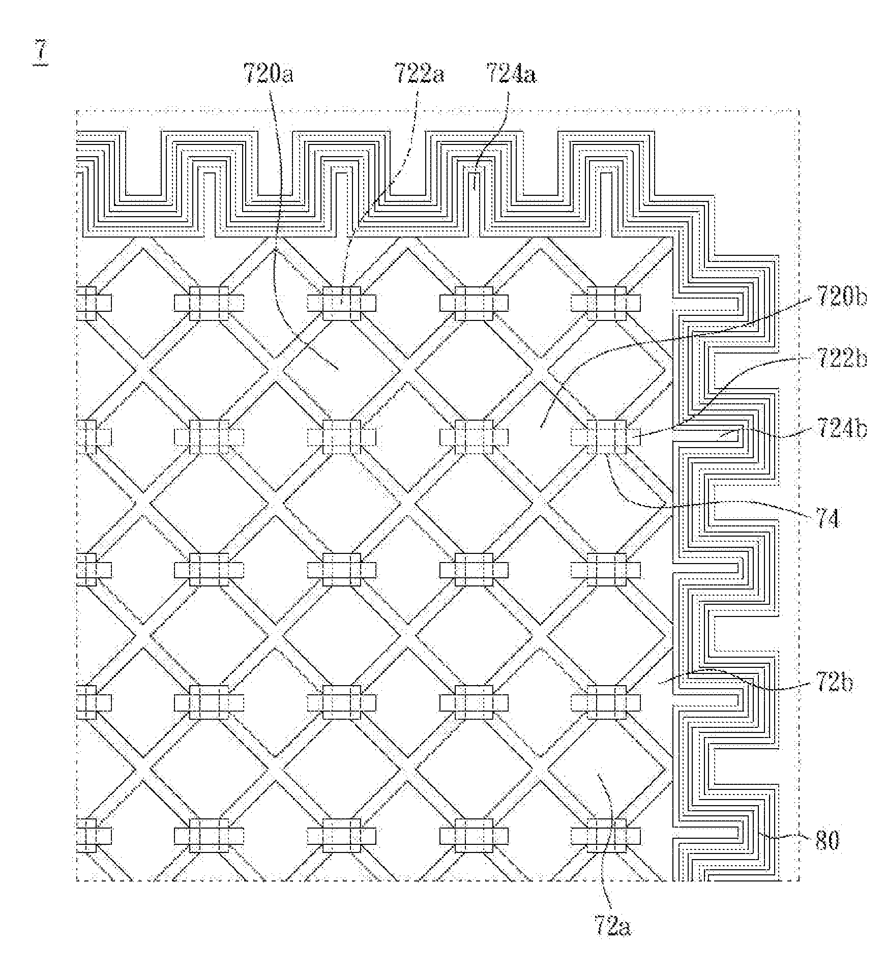
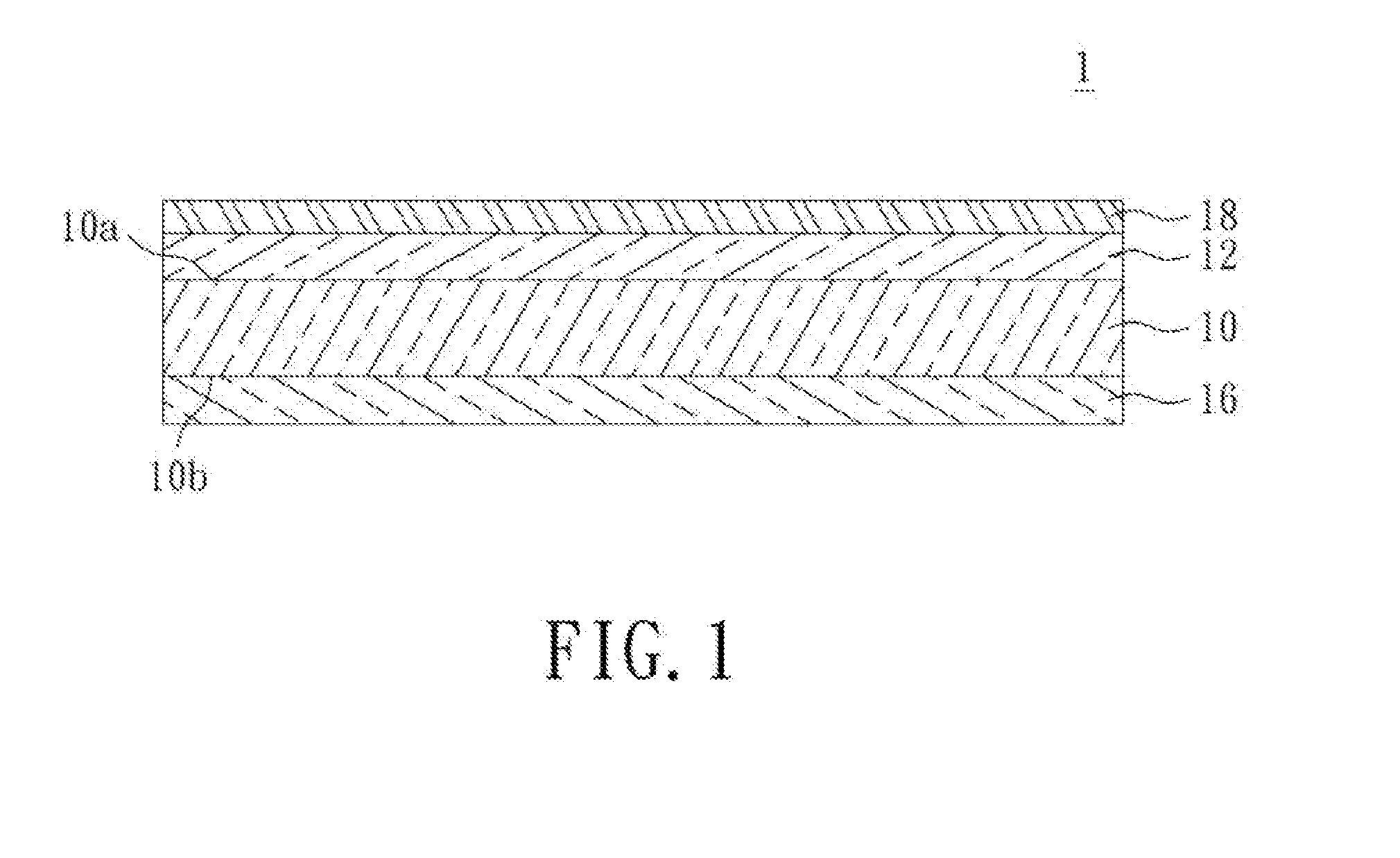
[0027]FIG. 1 is a sectional view of a touch panel with two conducting layers in accordance with an embodiment of the present disclosure. As shown in FIG. 1, the present disclosure demonstrates a structure with two conducting layers. A touch panel 1 comprises a substrate 10, a first conducting layer 12, a second conducting layer 16, and a protection layer 18. The substrate 10 is made of a material with high light transmittance and can be a planar or non-planar thin plate. For example, the substrate 10 can be made up of glass, plastic or mixed glass / plastic and formed into a glass thin plate or a flexible thin plate; the flexible thin plate can be made of polycarbonate (PC), polyester (PET), polymethyl methacrylate (PMMA) or cyclic olefin copolymer (COC).

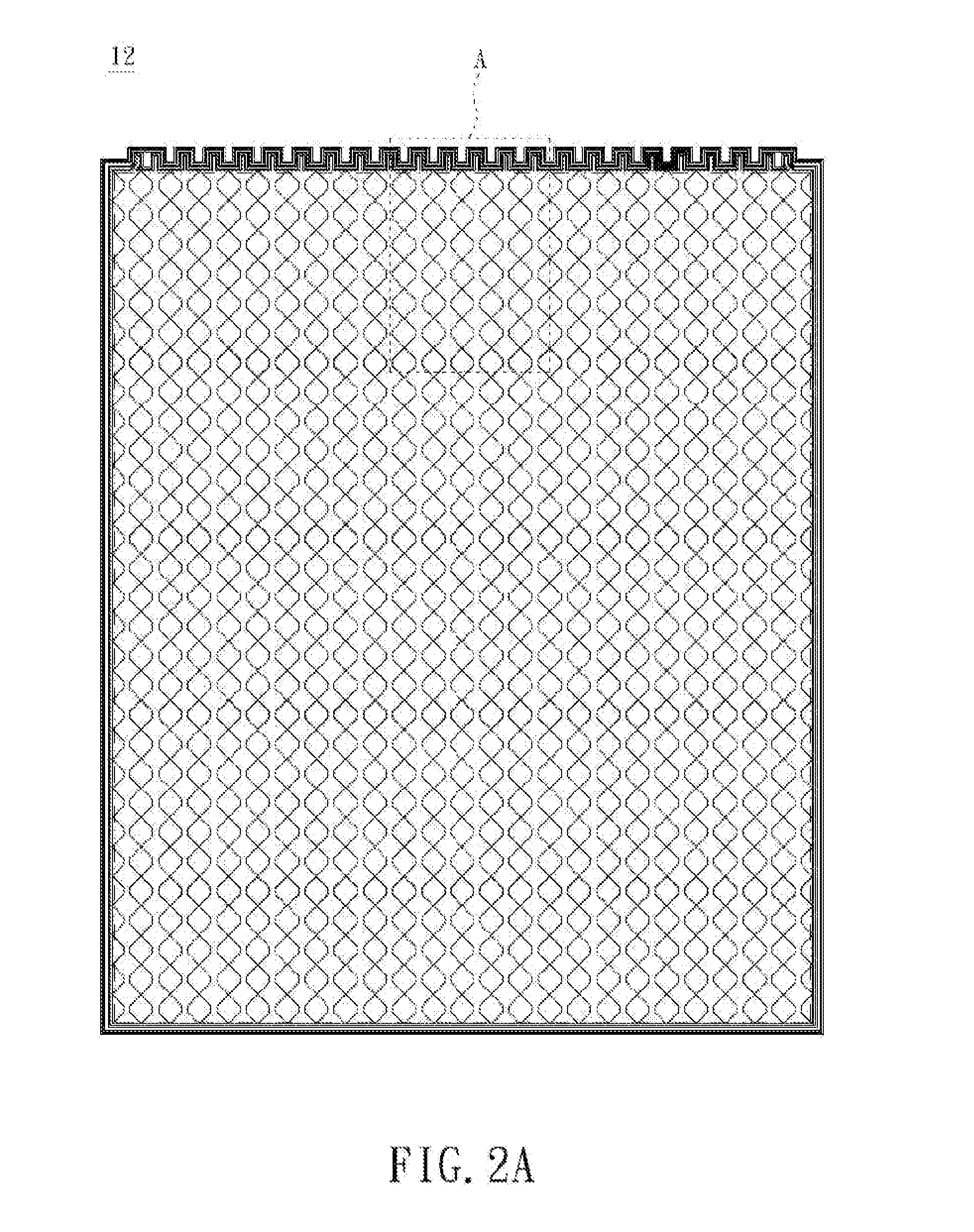
[0028]The first conducting layer 12 is formed on a first surface 10a of the substrate 10 and the second conducting layer 16 is formed on a second surface 10b of the substrate 10 such that the first conducting layer 12 is insulated fro...


PUM

PropertyMeasurementUnit
Timeaaaaaaaaaa
Wavelengthaaaaaaaaaa
Flexibilityaaaaaaaaaa

Abstract

The present disclosure discloses a touch panel, a touch electrode structure, and a manufacturing method thereof. The touch electrode structure comprises a plurality of first-axis sensing lines and at least one first laser etching line. The plurality of first-axis sensing lines are formed by laser etching a first conducting layer, wherein each first-axis sensing line at least has a first output pin. The first laser etching line is formed around the corresponding first output pin by laser etching the first conducting layer. Thus, the present disclosure can reduce overall production time by using a simplified manufacturing process in a laser etching process to form an improved touch electrode structure.

Description

[0001]This application claims the benefit of Chinese application No. 201110379425.4, filed on Nov. 9 2011.BACKGROUND OF THE INVENTION[0002]1. Field of the Invention[0003]The present disclosure relates to a touch technology, more specifically to a touch electrode structure, a method of manufacturing the same, and a touch panel applying the structure.[0004]2. Description of the Related Art[0005]Touch panels have been widely used, most typically, in smart phones and tablet PCs. Most smart phones and tablet PCs are equipped with a touch panel, which facilitates operation by a user and achieves an operation that is completely different from that of a keyboard. Touch panels are broadly classified into resistive touch panels, capacitive touch panels, acoustic wave touch panels, optical touch panels, and electromagnetic touch panels.[0006]Generally, a touch panel has uniaxial sensing lines or biaxial sensing lines. The uniaxial sensing lines can be designed into a single axis having a funct...

Claims


Application Information

Patent Timeline
IPC IPC(8): H01H13/704H01H11/00
CPCH01H11/00H01H13/704G06F3/0445G06F3/0446G06F2203/04103Y10T29/49105G06F3/041G06F2203/04111H01B5/14H01B13/00H03K17/962
Inventor JIANG, YAU-CHEN
Owner TPK TOUCH SOLUTIONS (XIAMEN) INC
Why Eureka
Try Eureka