Method for estimating the end of lifetime for a power semiconductor device

a technology of power semiconductors and end of life, which is applied in the direction of semiconductor operation lifetime testing, measurement devices, instruments, etc., can solve the problems of rendering the semiconductor device usable, and it is impossible to predict the end of life of the semiconductor device, so as to prolong the lifetime of the power device, simple and systematic, and minimal thermal stack temperature gradient

Active Publication Date: 2014-05-08
K B ELECTRONICS INC
View PDF8 Cites 17 Cited by
  • Summary
  • Abstract
  • Description
  • Claims
  • Application Information

AI Technical Summary

Benefits of technology

[0009]In case of a wind turbine the knowledge of the end of lifetime for a power device can prevent loss of production as the power device can be replaced and / or be de-rated in order to keep the power device in production until change of the device can be made. Further, it is noted that the power semiconductor device can be used in between the voltage drops are determined and after the end of lifetime is estimated. It is an advantage of the present invention that lifetime can be estimated with only a short non-operation period of the power semiconductor device. In other words the method is non-destructive for the power semiconductor device.
[0010]Power semiconductor device can be understood as a part of a power converter, such as a power inverter or power stack. The power semiconductor device can be build up of diodes, such as power silicon or silicon carbide diodes, or switches, such as MOSFET's, IGBT's, GTO's, IGCT's, thyristors or silicon carbide switches.
[0011]A power semiconductor device of a power converter are loaded differently during the lifetime of a power semiconductor device and it is impossible to produce all power semiconductors of one type, completely identical, which results in different electrical resistance over the power semiconductor device. Among other things, this has made it impossible to determine the end of lifetime for a power semiconductor device in the past. However, by use of the present invention this is now possible. The expression “not in operation” should be understood in such a way that the power semiconductor device is not performing the task that it is intended for in the system wherein it is installed. A power semiconductor device can be in operation or not in operation, when in operation the power semiconductor device converts power in the apparatus where it is installed and when not in operation the semiconductor does not convert power in the apparatus where it is installed. For example, a power semiconductor device in a power inverter, is not in operation when it is not actively conducting current to be converted. Alternatively one of the following words can be used, not in action, off-line or non production mode.
[0012]In a power device there can be one or more thermal stacks with power semiconductor material (also known as a power semiconductor chip or simply chip) thermally connected to a baseplate, the connection can be secured by isolation and solder. Further structural possibilities for thermal stacks in a power semiconductor device are known in the art, for example the thermal stack can be made without a baseplate. The baseplate can be made from copper or AlSiC and connected to a heat sink, such as a liquid cooling system. As there is a temperature gradient in the thermal stack when the power device is in operation, the temperature of the chip is not identical to the temperature of the liquid or the base plate. Therefore it is an advantage to perform the voltage measuring when the temperature is known and when the device is not in operation. This is because the temperature gradient in the thermal stack is minimal when the power semiconductor device is not in operation as no heat is produced in the silicon chip.
[0013]In an embodiment, the end of lifetime is established by comparing the plurality of determined voltage drops with a reference data set of voltage drops. Preferably, the reference data set is established via accelerated tests. This ensures a simple and systematic way of evaluating the end of lifetime. Alternatively, actual measurements from a similar power semiconductor device or theoretical calculated can be used as reference data. It is to be understood that every type and specific construction of a power device and converter design could require its specific reference data set.
[0014]Advantageously, the reference data set can be substituted with a new updated reference data set at any time. As the condition and the gradual wear out of the power semiconductor device changes over time it is an advantage to be able to update the reference data set at any time.

Problems solved by technology

This method is destructive and renders the semiconductor device usable.
Further, the method applies stress to an element of the semiconductor, such as a gate oxide film, which makes it impossible to predict the end of lifetime for the semiconductor device.

Method used


Image

  • Method for estimating the end of lifetime for a power semiconductor device
  • Method for estimating the end of lifetime for a power semiconductor device
  • Method for estimating the end of lifetime for a power semiconductor device

Examples


Embodiment Construction

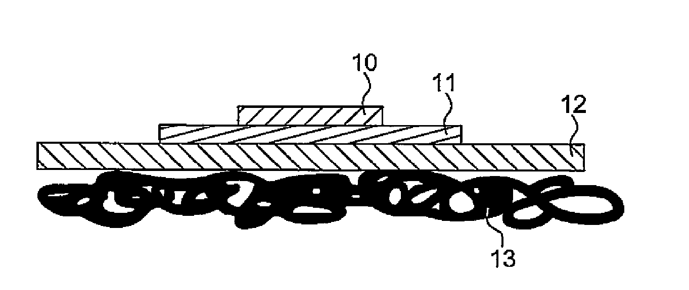
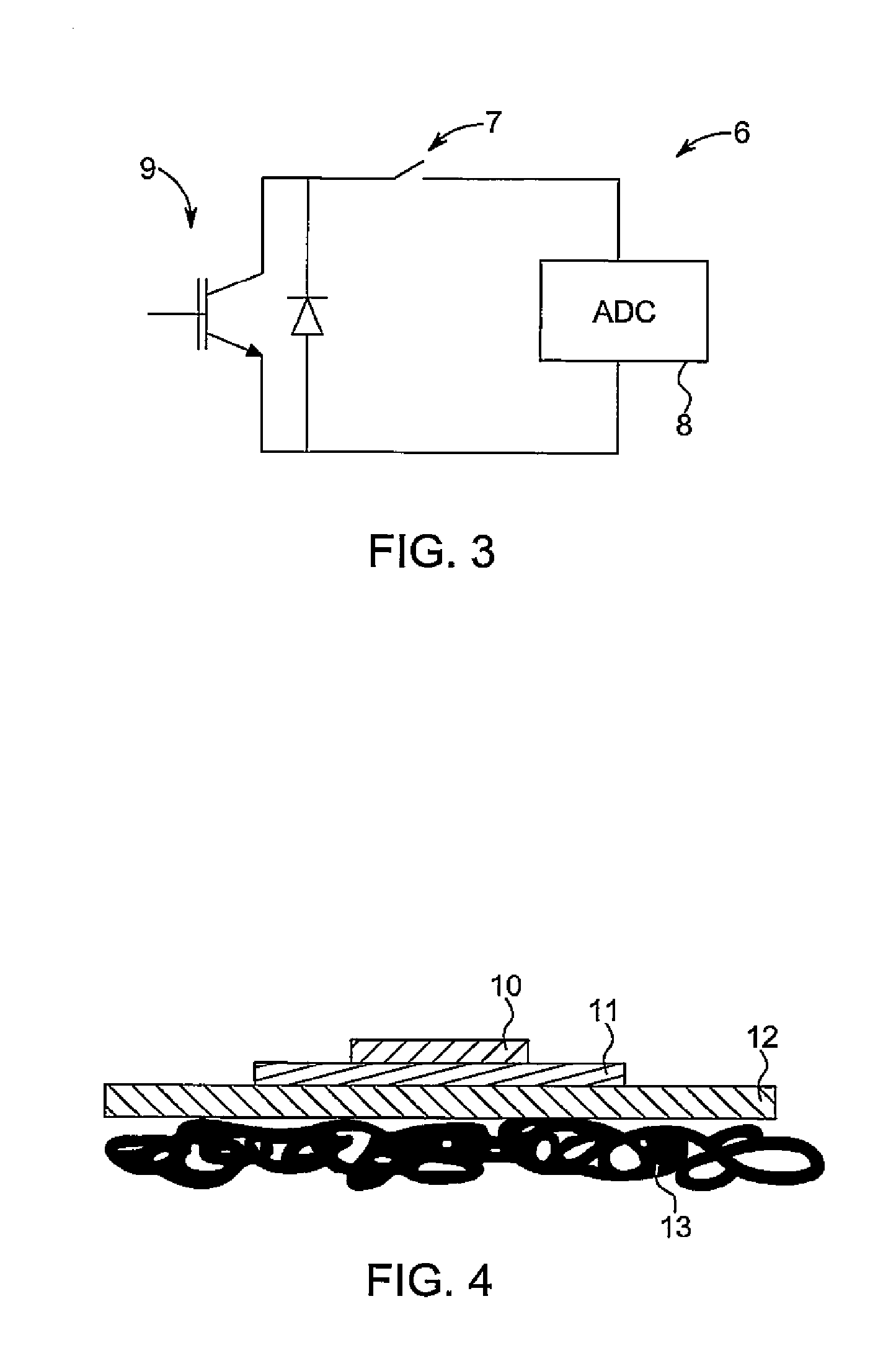
[0044]The invention relates to estimation of remaining or end of lifetime for power semiconductor devices being part of power converters, and for example being build up of active switches and / or diodes, for example: IGBT's, Thyristors, GTO's, MOSFET's, IGCT's, silicon carbide switches, power silicon diodes or power silicon carbide diodes. The estimation method is based on the establishment (e.g. measurement) of the voltage drop across the power device, when it is conducting a current. These voltage measurements are then stored and the end of lifetime is estimated on the basis of changes in the voltage drop as a function of the lifetime consumption by the power device.

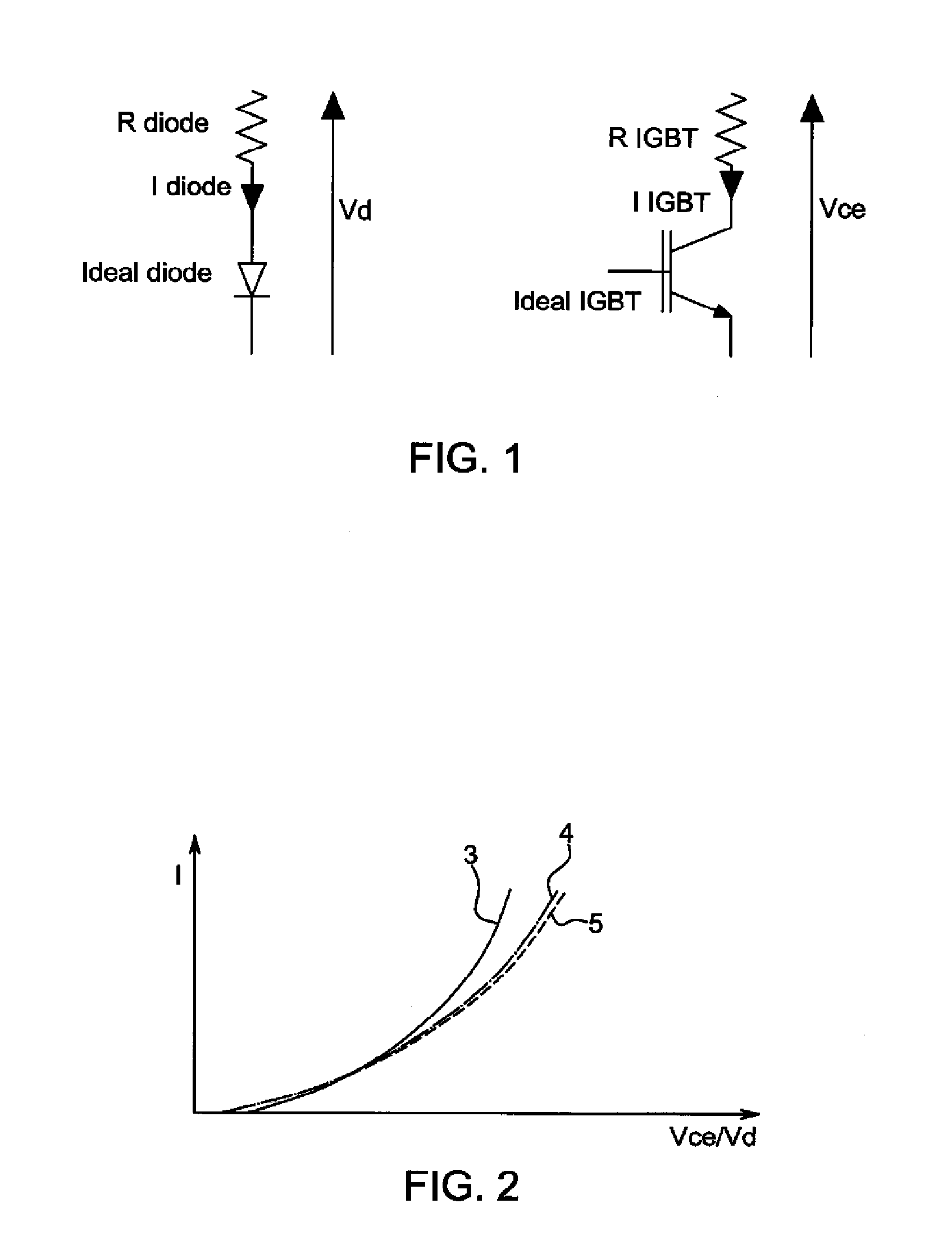
[0045]When current flows through the power device, such as a diode or an IGBT switch a voltage drop is generated across the component as shown in FIG. 1. The voltage drop can be divided into a voltage drop across a resistive part and voltage drop across the PN junction inside the semiconductor chips. Resistance lies in ...


PUM


Abstract

The invention regards an method for estimating the end of lifetime for a power semiconductor device, such as an IGBT power module, comprising the steps of; establishing the temperature of the power semiconductor device, determining the voltage drop over the power semiconductor device for at least one predetermined current where the current is applied when the power semiconductor device is not in operation, wherein the end of lifetime is established dependent on the change in a plurality of determined voltage drops.

Description

FIELD OF INVENTION[0001]The invention relates to a method and an apparatus for estimating the end of lifetime for a power semiconductor device and a wind turbine using the method or comprising the apparatus.BACKGROUND OF THE INVENTION[0002]Power semiconductor devices, also known as power devices, are known in the art and used as switches or rectifiers in power electronic circuits. In wind turbines power semiconductor devices can be used to connect the generator with the grid. In some wind turbines power converters (comprising semiconductor devices) controls the power flow to the grid.[0003]It is known in the art that power semiconductor device wear out due to mechanical and thermal stress, therefore it is desirable to be able to estimate the end of lifetime or remaining lifetime for a power semiconductor device. This makes it possible, for example, to plan the replacement of the devices before a critical failure.[0004]U.S. Pat. No. 5,877,419 discloses a method for estimating the ser...

Claims


Application Information

Patent Timeline
Patent Type & Authority Applications(United States)
IPC IPC(8): G01R31/26
CPCG01R31/2642G01R31/2608G01R31/2817
Inventor THOGERSEN, PAUL BACHRANNESTAD, BJORN
Owner K B ELECTRONICS INC
Why Eureka
Try Eureka