Device for handling microfluids and a method of manufacturing a device for handling microfluids
- Summary
- Abstract
- Description
- Claims
- Application Information
AI Technical Summary
Benefits of technology
Problems solved by technology
Method used
Image

Examples
Embodiment Construction
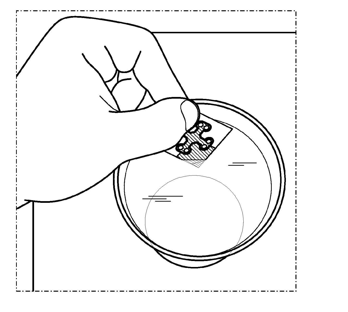
[0037]FIG. 1 presents the use of a device (which in an advantageous embodiment is a test platform) for handling microfluids. In step 101 the sample is absorbed into the device. In step 103 the sample travels in the microfluidic channels of the device. In step 105 the sample is dispensed exactly to the test zones in the device. In step 107 the sample is analyzed using the test zones.
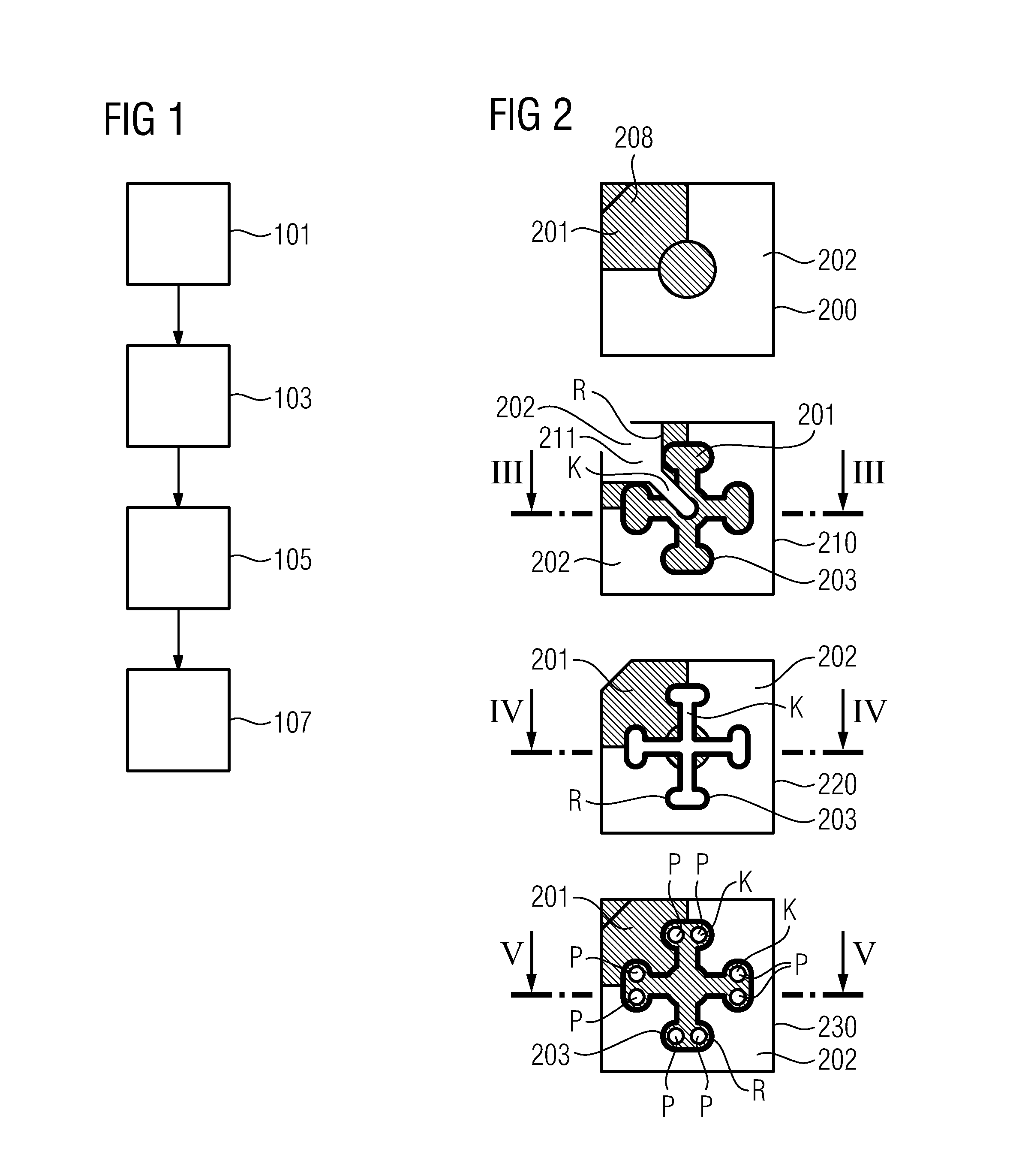
[0038]FIG. 6 presents the process of manufacturing a device for handling microfluids. In step 601 hydrophobic regions are created. In the optional step 603 the layers are further processed. In the optional step 605 the test zones are processed to be ready for analysis. In step 611 the layers are joined together. In step 613 the devices are cut away from each other and in step 615 the ready devices are packed.
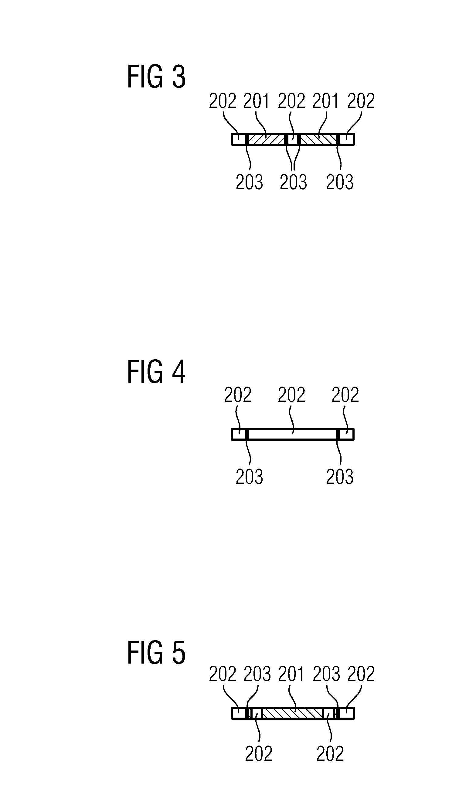
[0039]The hydrophobic regions of step 601 are created as follows:
[0040]Wax 201 is brought to sheet 700 in the way that is apparent in FIG. 7 by printing a desired pattern on it with a Xerox Corp. Soli...
PUM
| Property | Measurement | Unit |
|---|---|---|
| Thickness | aaaaa | aaaaa |
| Solubility (mass) | aaaaa | aaaaa |
| Adhesivity | aaaaa | aaaaa |
Abstract
Description
Claims
Application Information
 - R&D Engineer
- R&D Manager
- IP Professional
- Industry Leading Data Capabilities
- Powerful AI technology
- Patent DNA Extraction
Browse by: Latest US Patents, China's latest patents, Technical Efficacy Thesaurus, Application Domain, Technology Topic.
© 2024 PatSnap. All rights reserved.Legal|Privacy policy|Modern Slavery Act Transparency Statement|Sitemap