Display device
- Summary
- Abstract
- Description
- Claims
- Application Information
AI Technical Summary
Benefits of technology
Problems solved by technology
Method used
Image

Examples
embodiment 1
[0082]The following description discusses Embodiment 1 of the present invention with reference to FIGS. 1 to 10.
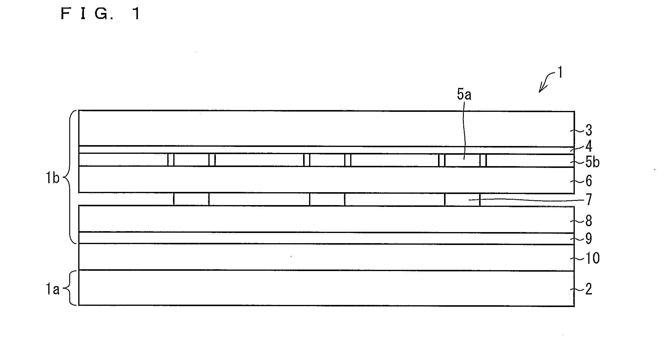
[0083]FIG. 1 schematically illustrates a configuration of a liquid crystal display device 1 which includes an in-cell, mutual-capacitance touch panel.
[0084]As illustrated in FIG. 1, the liquid crystal display device 1 includes a TFT substrate 1a, a color filter substrate 1b, and a liquid crystal layer sandwiched between the TFT substrate 1a and the color filter substrate 1b.
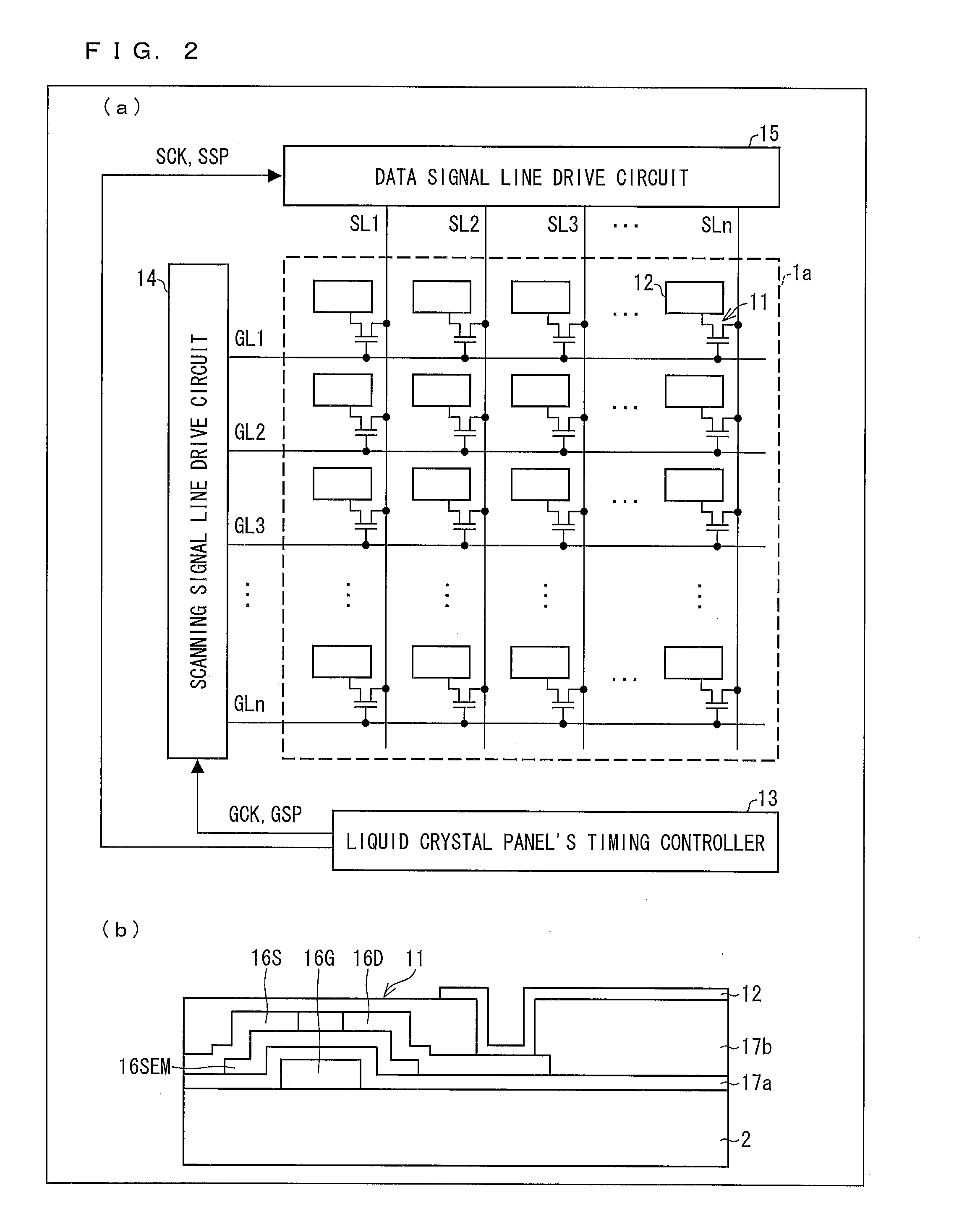
[0085]The TFT substrate 1a is constituted by an insulating substrate 2 which has pixel TFT elements (not illustrated, described later in detail) on its surface facing the liquid crystal layer 10.
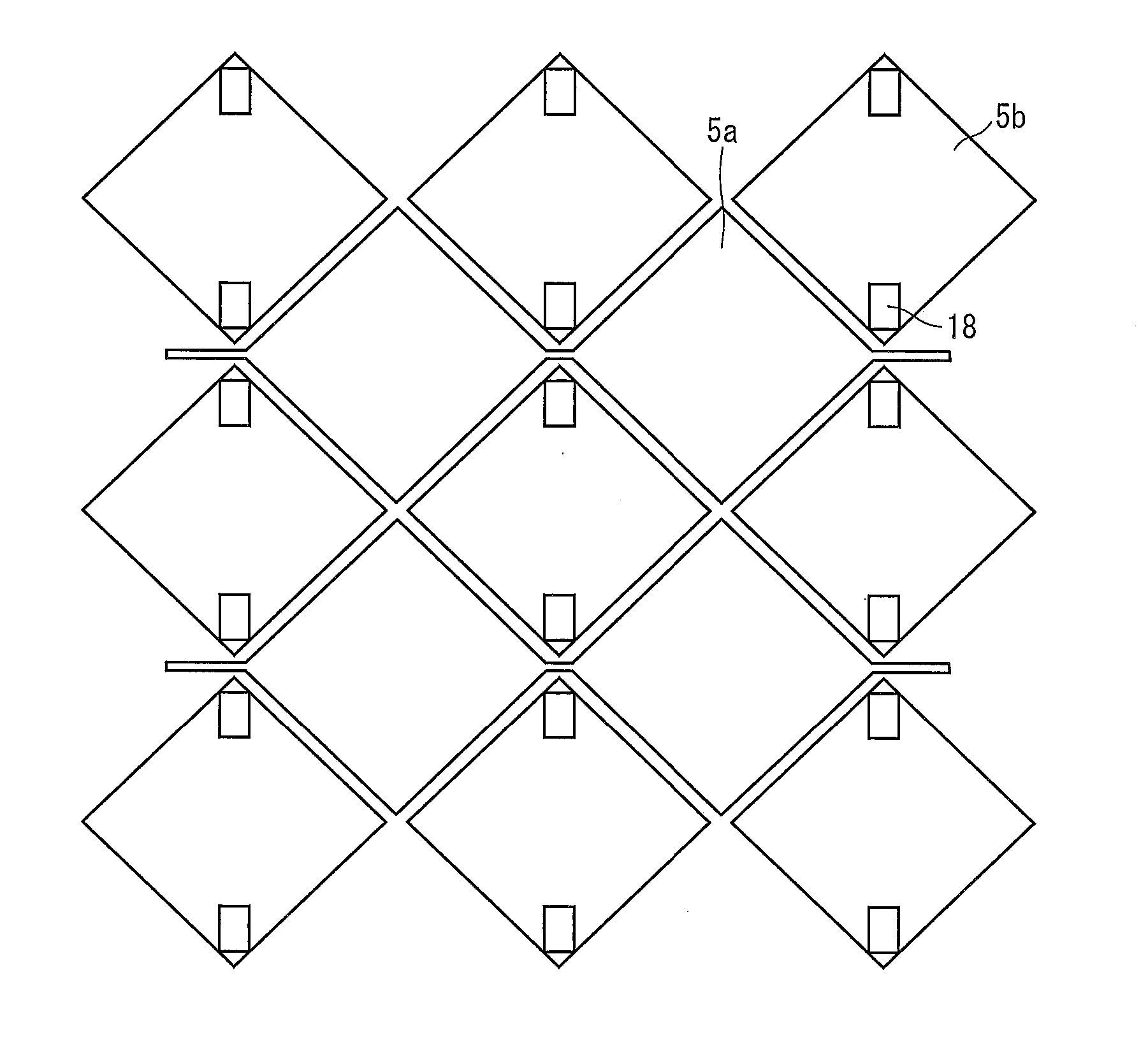
[0086]On the other hand, the color filter substrate 1b is constituted by an insulating substrate 3 which has, on its surface facing the liquid crystal layer 10, a black matrix / color filter layer 4, a layer of drive electrodes 5a and sense electrodes 5b, a first insulating layer 6, a layer of bridging electrodes...
embodiment 2
[0157]The following description discusses Embodiment 2 of the present invention with reference to FIGS. 11 to 13. A liquid crystal display device of the present embodiment includes, for a color filter substrates 1c or 1d, a liquid crystal panel's timing controller and a touch panel's control circuit usable for various driving methods as described in Embodiment 1. The liquid crystal display device of the present embodiment is different from Embodiment 1 in that, also for the liquid crystal panel including the touch panel, a metal conductive layer 27 is provided which is electrically connected to a common electrode layer 9 to reduce resistance of the common electrode layer 9. The other configurations of the liquid crystal display device of the present embodiment are as described in Embodiment 1. For convenience of description, members having functions identical to those illustrated in the drawings of Embodiment 1 are assigned identical referential numerals, and their descriptions are ...
embodiment 3
[0174]The following description discusses Embodiment 3 of the present invention with reference to FIGS. 14 to 19. The present embodiment is different from Embodiments 1 and 2 in that the touch panel of the liquid crystal display device used in Embodiment 2 employs parallel driving. The other configurations are as described in Embodiments 1 and 2. For convenience of description, members having functions identical to those illustrated in the drawings of Embodiments 1 and 2 are assigned identical referential numerals, and their descriptions are omitted here.
[0175]FIG. 14 schematically illustrates a configuration of a touch panel included in a liquid crystal display device of the present embodiment.
[0176]As shown in FIG. 14, a drive line drive circuit 30 includes a drive line selection circuit 31 and an M-sequence generating circuit 32. A sense line drive circuit 33 includes a sense line selection circuit 34, an amplifier circuit 35, an A / D converter circuit 36, a correlation calculatio...
PUM
 Abstract
Description
Claims
Application Information
 - R&D
- Intellectual Property
- Life Sciences
- Materials
- Tech Scout
- Unparalleled Data Quality
- Higher Quality Content
- 60% Fewer Hallucinations
Browse by: Latest US Patents, China's latest patents, Technical Efficacy Thesaurus, Application Domain, Technology Topic, Popular Technical Reports.
© 2025 PatSnap. All rights reserved.Legal|Privacy policy|Modern Slavery Act Transparency Statement|Sitemap|About US| Contact US: help@patsnap.com