Semiconductor apparatus

a technology of semiconductor devices and fuses, which is applied in the direction of electrical devices, semiconductor devices, and/or solid-state device details, etc., can solve the problems of short circuits of cut fuses, and deteriorating reliability of semiconductor devices, so as to improve reliability

Active Publication Date: 2014-06-05
SK HYNIX INC
View PDF0 Cites 2 Cited by
  • Summary
  • Abstract
  • Description
  • Claims
  • Application Information

AI Technical Summary

Benefits of technology

[0007]Various embodiments are directed to a semiconductor apparatus capable of improving reliability.

Problems solved by technology

In such procedures, a fail is likely to occur in that a fuse of the semiconductor apparatus is changed from a cut state into an uncut state, and thus, a problem is caused in that the reliability of the semiconductor apparatus deteriorates.
Due to migration of the ions, the anode electrode of the fuse is electrically connected to the cathode electrode of the fuse, thus, the cut fuses are likely to be short-circuited.
That is to say, as a fail occurs in that the cut fuse is changed into an uncut state, the reliability of the semiconductor apparatus may deteriorate.

Method used


Image

  • Semiconductor apparatus
  • Semiconductor apparatus
  • Semiconductor apparatus

Examples


Embodiment Construction

[0031]Hereafter, various embodiments will be described in detail with reference to the accompanying drawings.

[0032]It is to be understood herein that the drawings are not necessarily to scale and in some instances proportions may have been exaggerated in order to more clearly depict certain features of the invention. Also, the same reference numerals or the same reference designators may denote the same elements throughout the specification.

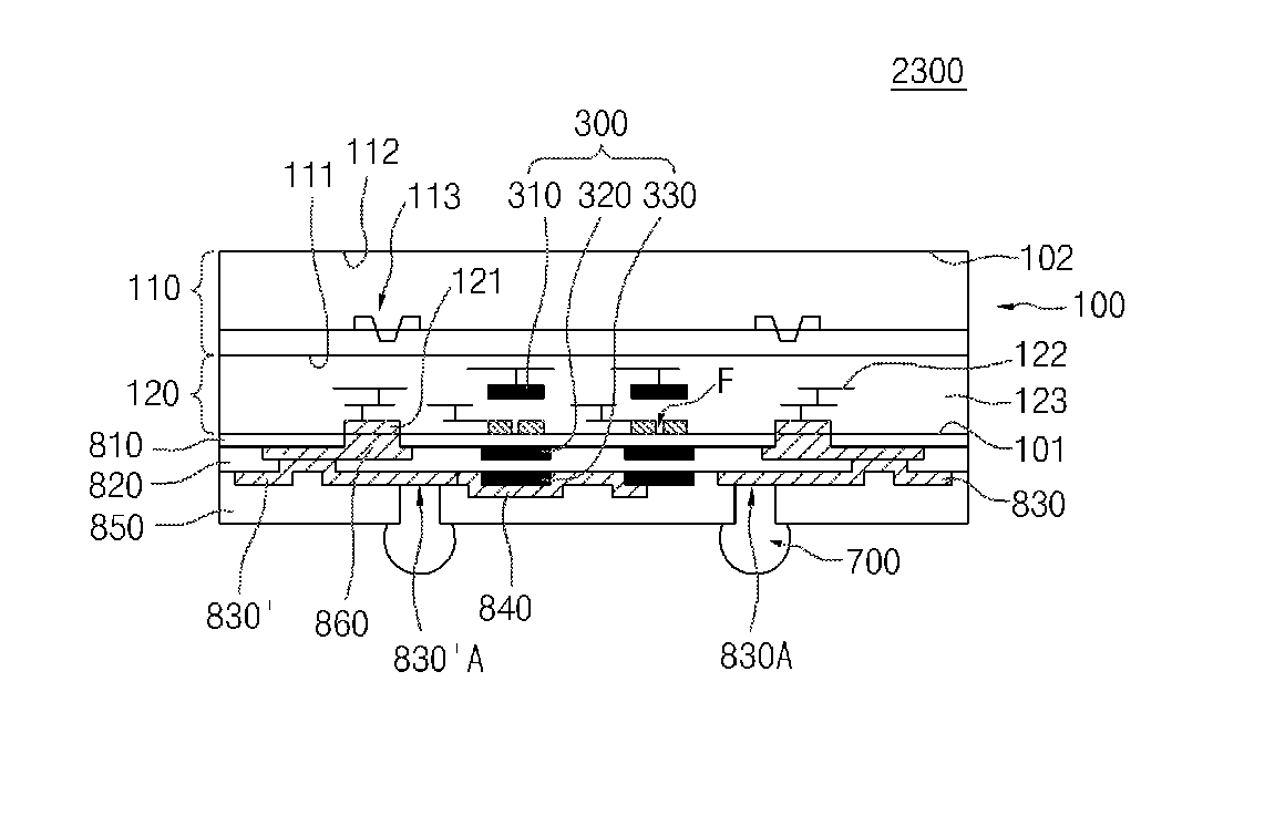
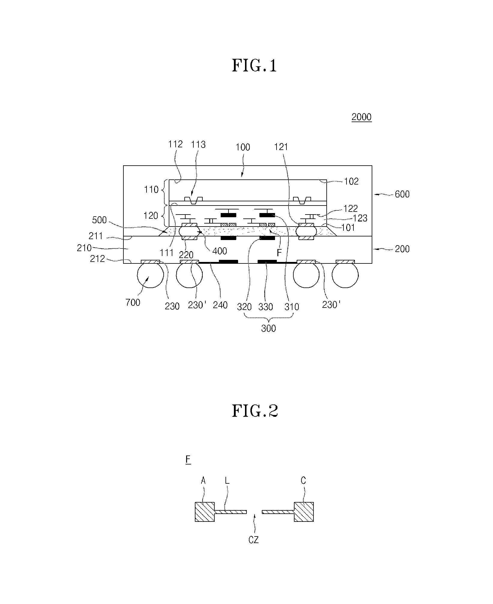
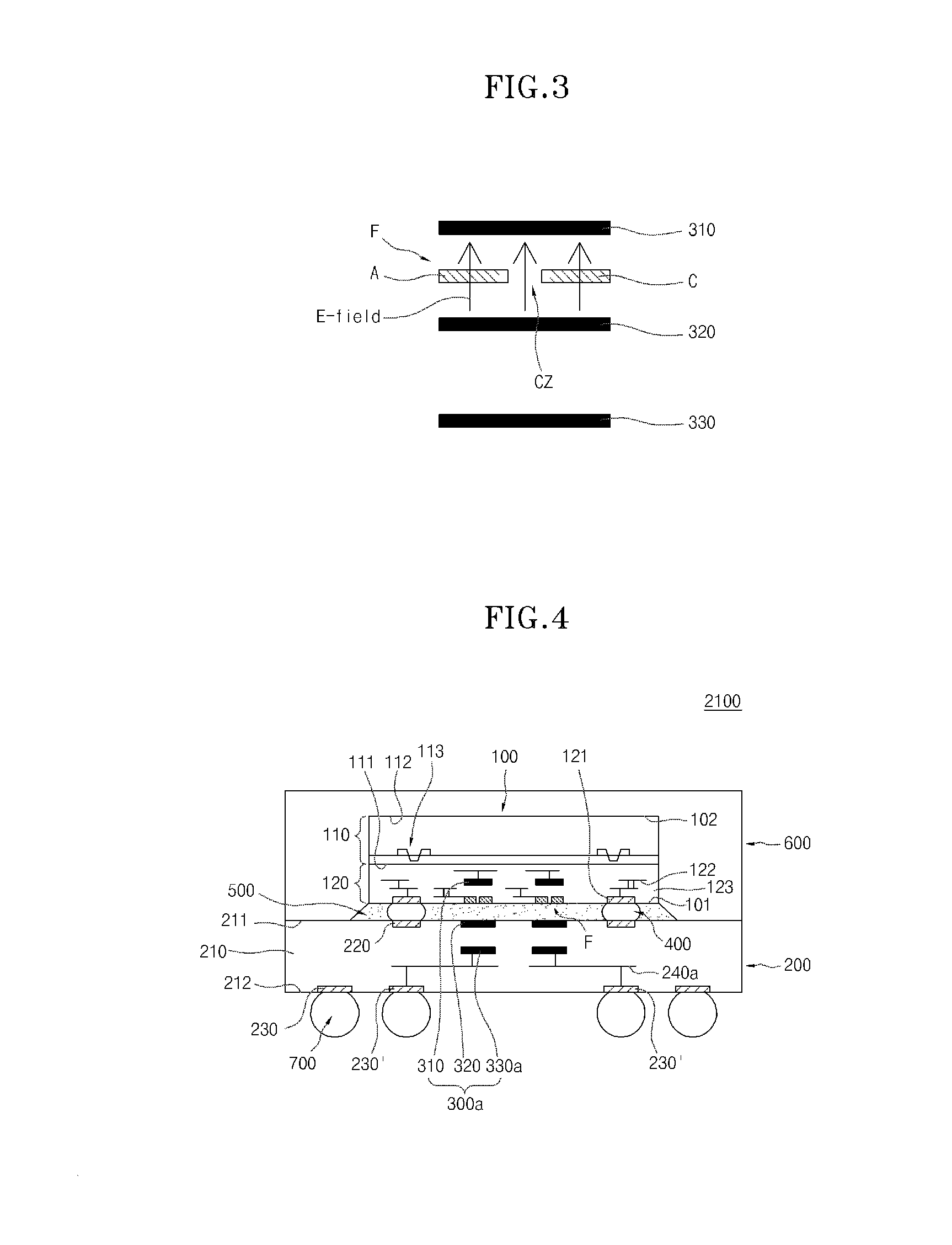
[0033]Referring to FIG. 1, a semiconductor apparatus 2000 may include a semiconductor chip 100, a printed circuit board 200, and migration preventing modules 300. The semiconductor apparatus may further include conductive connection members 400, an underfill member 500, a molding part 600, and external connection terminals 700.

[0034]The semiconductor chip 100 may have one surface 101 on which fuses F are formed and the other surface 102 which faces away from the one surface 101. The semiconductor chip 100 may include a substrate 110 having the ot...


PUM


Abstract

A semiconductor apparatus includes a semiconductor chip formed with cut fuses over one surface thereof; and migration preventing modules preventing occurrence of a phenomenon in which metal ions of the fuses migrate to cut zones of the fuses; each migration preventing module including: a ground electrode formed in the semiconductor chip to face the fuse with a first insulation member interposed therebetween; a floating electrode formed over the fuse with a second insulation member interposed therebetween to face the ground electrode with the fuse interposed therebetween; and a power supply electrode formed over the floating electrode with a third insulation member interposed therebetween.

Description

CROSS-REFERENCE TO RELATED APPLICATION[0001]The present application claims priority under U.S.C 119(a) to Korean Patent Application Number 10-2012-0138754 filed in the Korean Intellectual Property Office on Dec. 3, 2012, which is incorporated herein by reference in its entirety.BACKGROUND[0002]1. Field of Invention[0003]The present invention generally relates to a semiconductor apparatus, and more particularly, to a semiconductor apparatus having fuses.[0004]2. Description of the Related Art[0005]A semiconductor apparatus undergoes procedures such as THB (temperature humidity bias) and HAST (high acceleration stress test) to measure a reliability of the semiconductor apparatus. In such procedures, a fail is likely to occur in that a fuse of the semiconductor apparatus is changed from a cut state into an uncut state, and thus, a problem is caused in that the reliability of the semiconductor apparatus deteriorates.[0006]In detail, TBH and HAST are procedures for a testing reliability ...

Claims


Application Information

Patent Timeline
Patent Type & Authority Applications(United States)
IPC IPC(8): H01L23/525
CPCH01L23/5256H01L23/564H01L2224/16225H01L2224/32225H01L2224/48091H01L2224/4824H01L2224/73204H01L2224/73215H01L2924/15311H01L2924/00014H01L2924/00H01L23/62
Inventor KIM, JAE MINPARK, MYUNG GUN
Owner SK HYNIX INC
Why Eureka
Try Eureka