Body voltage sensing based short pulse reading circuit

a sensing circuit and body voltage technology, applied in the field of resistance sensing based random access memory (ram) devices, can solve the problems of substantially outperforming the reference design in sensing speed and read margin (rm), and achieve the effect of reducing read disturbance probability, high sensing margin (sm), and high sensing speed

Inactive Publication Date: 2014-06-05
RGT UNIV OF CALIFORNIA
View PDF2 Cites 16 Cited by
  • Summary
  • Abstract
  • Description
  • Claims
  • Application Information

AI Technical Summary

Benefits of technology

[0015]By way of example and not limitation, this SPR circuit is simulated in 65 nm Spice simulations. The following sections analyze the read margin (RM) and performance of the inventive BVSC and compare them to those of the two reference designs, specifically CMSC and SPSC. Departing from CMSC and SPSC designs, BVSC utilizes the unique small signal resistance of the body-connected load to achieve higher sensing margin (SM), or equivalently, higher sensing speed for the same SM. This leads to a shorter sensing current pulse applied on the resistive storage device, which significantly reduces read disturbance probability, thus increasing read reliability.

Problems solved by technology

As a result, BVSC substantially outperforms the reference designs in sensing speed and read margin (RM).

Method used


Image

  • Body voltage sensing based short pulse reading circuit
  • Body voltage sensing based short pulse reading circuit
  • Body voltage sensing based short pulse reading circuit

Examples


Embodiment Construction

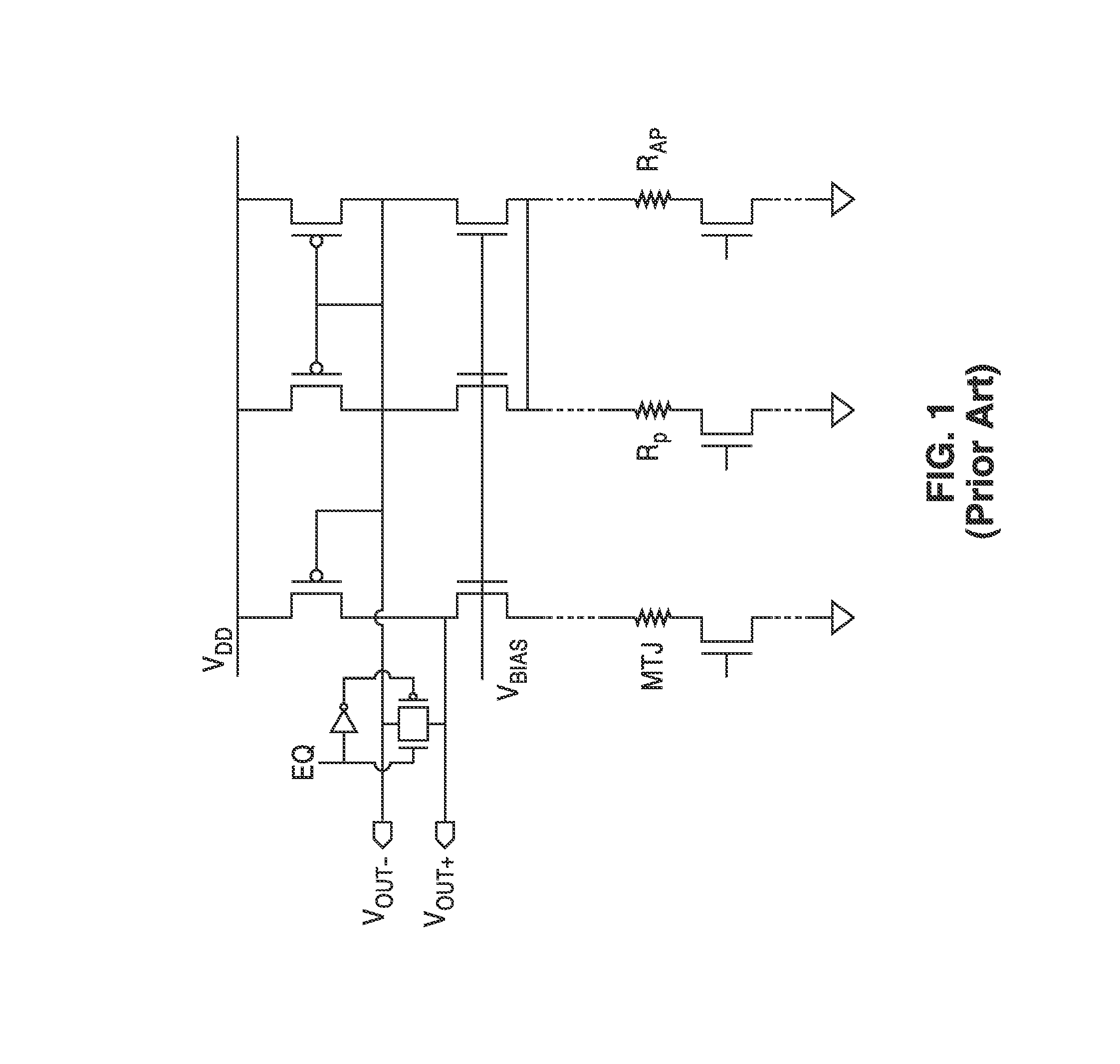
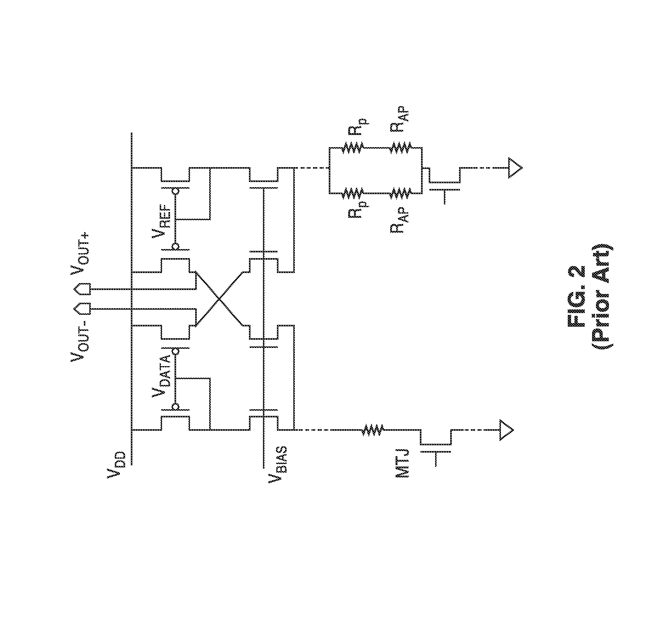
1. High Speed Reading of STT-RAM

[0031]1.1. MTJ Switching

[0032]In this section, the STT-RAM is used as an application example of the inventive reading circuit, however, the inventive read circuit is not limited to application within STT-RAM devices. One of ordinary skill in the art will recognize that the inventive reading circuit may be applied in any memory device in which the memory states are determined in response to different resistance levels.

[0033]The key memory device in STT-RAM devices is the magnetic tunnel junction (MTJ), which has two ferromagnetic layers separated by a thin, nonconductive tunneling barrier. The thicker layer, called the fixed layer (or pinned layer), has a certain layer stack structure fixing its magnetic orientation. The thinner layer, whose magnetic orientation can be changed freely, is called the free layer. The MTJ exhibits two resistive states determined by the relative magnetization directions of the fixed and the free layers: a parallel (P) orien...


PUM


Abstract

As memory geometries continue to scale down, current density of magnetic tunnel junctions (MTJs) make conventional low current reading scheme problematic with regard to performance and reliability. A body-voltage sense circuit (BVSC) short pulse reading (SPR) circuit is described using body connected load transistors and a novel sensing circuit with second stage amplifier which allows for very short read pulses providing much higher read margins, less sensing time, and shorter sensing current pulses. Simulation results (using 65-nm CMOS model SPICE simulations) show that our technique can achieve 550 mV of read margin at 1 ns performance under a 1V supply voltage, which is greater than reference designs achieve at 5 ns performance.

Description

CROSS-REFERENCE TO RELATED APPLICATIONS[0001]This application is a 35 U.S.C. §111(a) continuation of PCT international application number PCT / US2012 / 056136 filed on Sep. 19, 2012, incorporated herein by reference in its entirety, which is a nonprovisional of U.S. provisional patent application Ser. No. 61 / 536,164 filed on Sep. 19, 2011, incorporated herein by reference in its entirety. Priority is claimed to each of the foregoing applications.[0002]The above-referenced PCT international application was published as PCT International Publication No. WO 2013 / 043738 on Mar. 28, 2013, which publication is incorporated herein by reference in its entirety.STATEMENT REGARDING FEDERALLY SPONSORED RESEARCH OR DEVELOPMENT[0003]This invention was made with Government support of Grant Number HR0011-09-C-0114, awarded by the Defense Advanced Research Projects Agency. The Government has certain rights in the invention.INCORPORATION-BY-REFERENCE OF MATERIAL SUBMITTED IN A COMPUTER PROGRAM APPENDIX...

Claims


Application Information

Patent Timeline
Patent Type & Authority Applications(United States)
IPC IPC(8): G11C11/16
CPCG11C11/1673G11C13/0004G11C13/0007G11C13/004G11C2013/0054G11C7/062G11C2207/063G11C11/16
Inventor WANG, KANG-LUNGYANG, CHIH-KONG K.MARKOVIC, DEJANREN, FENGBO
Owner RGT UNIV OF CALIFORNIA
Why Eureka
Try Eureka