Eureka AIR delivers breakthrough ideas for toughest innovation challenges, trusted by R&D personnel around the world.

Method for manufacturing semiconductor device

a manufacturing method and semiconductor technology, applied in the direction of semiconductor devices, basic electric elements, electrical appliances, etc., can solve the problems of electric characteristics defects of transistors, and achieve the effect of improving the reliability the electric characteristics of the semiconductor device using the oxide semiconductor

Active Publication Date: 2014-06-05
SEMICON ENERGY LAB CO LTD
View PDF2 Cites 60 Cited by
  • Summary
  • Abstract
  • Description
  • Claims
  • Application Information

AI Technical Summary

Benefits of technology

The present invention improves the electric and reliability of semiconductor devices using oxide semiconductor by controlling oxygen in the semiconductor film and reducing oxygen vacancies in the oxide film. This results in better control of the transistor's threshold voltage and reduced off-state current. Additionally, the transistor can be controlled to prevent it from becoming normally-on and to change or decrease its threshold voltage, providing further reliability and efficiency improvements.

Problems solved by technology

In a transistor using an oxide semiconductor, oxygen vacancies (oxygen defects) which are one of causes of localized levels in an oxide semiconductor film cause defects of electric characteristics of the transistor.

Method used


Image

  • Method for manufacturing semiconductor device
  • Method for manufacturing semiconductor device
  • Method for manufacturing semiconductor device

Examples


embodiment 1

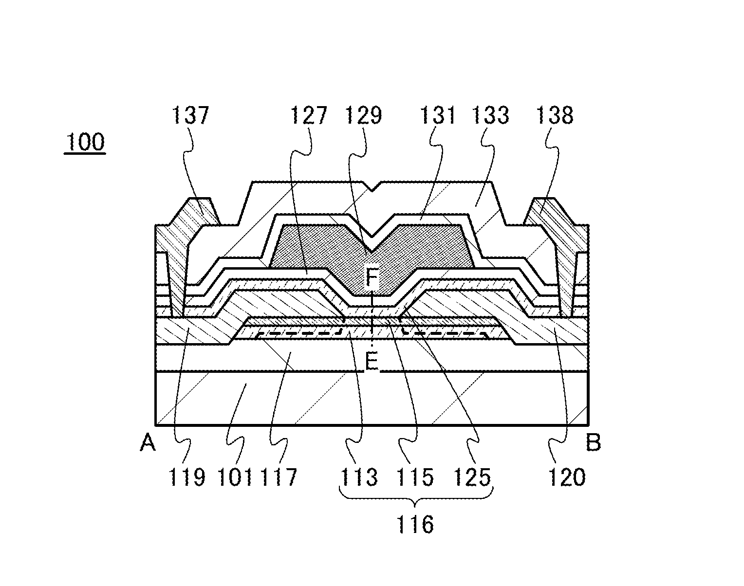
[0063]The threshold voltage of a transistor using an oxide semiconductor film with oxygen vacancies easily shifts negatively, and such a transistor tends to be normally-on. This is because electric charges are generated owing to oxygen vacancies in the oxide semiconductor, and the resistance is reduced. In addition, a transistor using an oxide semiconductor film with oxygen vacancies has such a problem that the electric characteristics, typically, the threshold voltage, are changed with time or changed by a stress test (typically, a gate bias-temperature (BT) stress test under light irradiation). In this embodiment, a highly reliable semiconductor device in which a change in threshold voltage is small and a manufacturing method thereof will be described. Further, a semiconductor device with excellent electric characteristics and a manufacturing method thereof will be described.

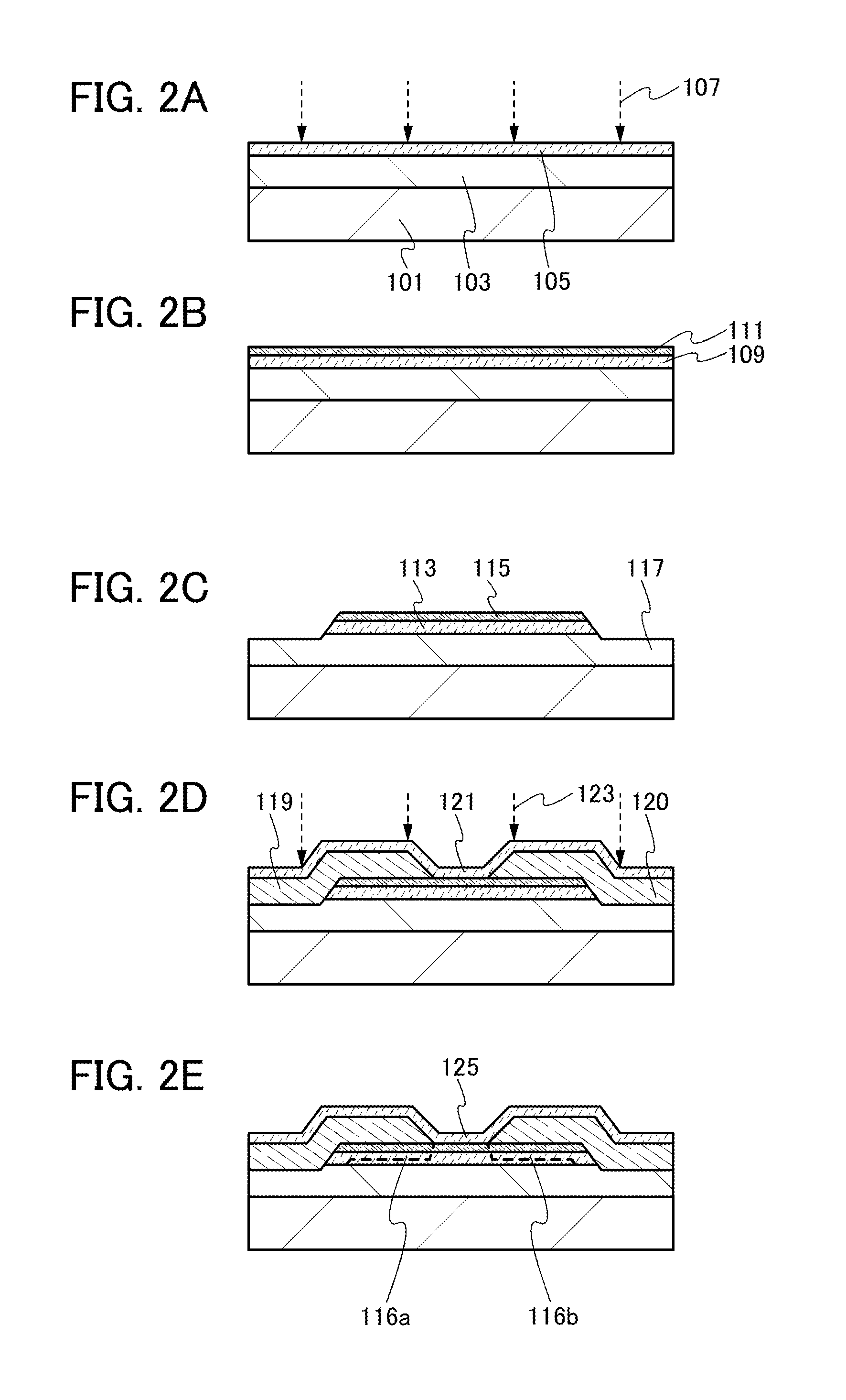
[0064]In this embodiment, a method for manufacturing a top-gate transistor is described.

[0065]FIGS. 1A to 1...

modification example 6

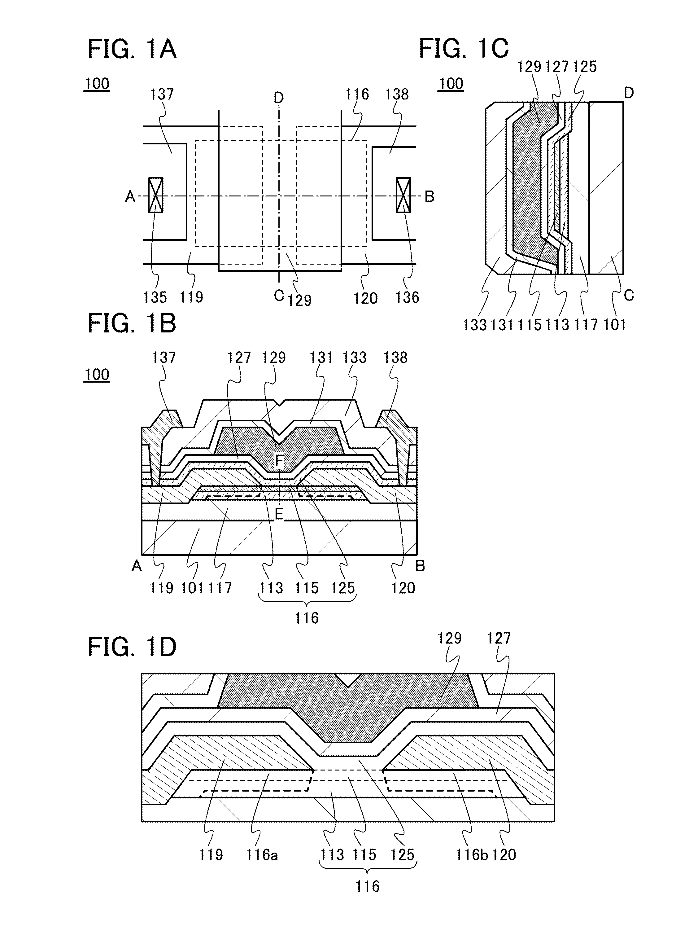
[0224]In the transistor in this embodiment, the pair of electrodes 119 and 120 is provided between the oxide semiconductor film 115 and the oxide film 125; however, the pair of electrodes 119 and 120 may be provided between the oxide insulating film 117 and the oxide film 113.

modification example 7

[0225]An insulating film that can be used as the oxide insulating film 117 functioning as a base insulating film in this embodiment is described below.

[0226]The oxide insulating film 117 can be formed using an oxide insulating film whose oxygen content is in excess of that in the stoichiometric composition. In other words, an oxide insulating film from which part of contained oxygen is released by heating can be formed. With use of such a film, the oxygen in the oxide insulating film 117 is transferred to the oxide semiconductor film 115; thus, the density of defect levels at the interface between the oxide insulating film 117 and the oxide film 113 can be reduced, and oxygen vacancies can be further reduced by filling oxygen vacancies in the oxide semiconductor film 115. For example, when an oxide insulating film having the following feature is used, the density of defect levels at the interface between the oxide insulating film 117 and the oxide film 113 can be decreased and oxyge...


PUM


Abstract

To improve electric characteristics of a semiconductor device including an oxide semiconductor. Alternatively, to improve reliability of a semiconductor device including an oxide semiconductor. In a transistor including a first oxide film, an oxide semiconductor film, a pair of electrodes in contact with the oxide semiconductor film, and a second oxide film in contact with the oxide semiconductor film and the pair of electrodes, oxygen is added to the first oxide film and the second oxide film in contact with the oxide semiconductor film and the pair of electrodes, so that oxygen vacancies are reduced. The oxygen is diffused to the oxide semiconductor film by heat treatment or the like; thus, oxygen vacancies in the oxide semiconductor film are reduced.

Description

BACKGROUND OF THE INVENTION[0001]1. Field of the Invention[0002]The present invention relates to an object, a process (including a method and a manufacturing method), a machine, a manufacture, or a composition of matter. In particular, the present invention relates to a semiconductor device, a display device, a light-emitting device, a driving method thereof, a manufacturing method thereof, or the like. In particular, the present invention relates to a semiconductor device, a display device, a light-emitting device, or the like including an oxide semiconductor.[0003]In this specification, a semiconductor device includes a device which can function by utilizing electronic characteristics of a semiconductor in its category, and for example, an electro-optic device, a semiconductor circuit, and an electric appliance are included in the category of the semiconductor device.[0004]2. Description of the Related Art[0005]Transistors used for most flat panel displays typified by a liquid cry...

Claims


Application Information

Patent Timeline
Patent Type & Authority Applications(United States)
IPC IPC(8): H01L21/02H01L29/66
CPCH01L29/7869H01L21/02488H01L21/02554H01L21/02565H01L21/02658H01L29/78618H01L29/78696
Inventor YAMAZAKI, SHUNPEI
Owner SEMICON ENERGY LAB CO LTD
Why Eureka
Eureka Blog
Learn More