Method for forming copper wiring

a technology of copper wiring and forming method, which is applied in the direction of resistive material coating, semiconductor/solid-state device details, superimposed coating process, etc., can solve the problems of difficult to obtain dense and continuous mn film, and achieve the effect of low resistance of cu wiring and good fillability

Active Publication Date: 2014-06-12
TOKYO ELECTRON LTD
View PDF7 Cites 9 Cited by
  • Summary
  • Abstract
  • Description
  • Claims
  • Application Information

AI Technical Summary

Benefits of technology

[0007]In view of the above, the present invention provides a Cu wiring forming method capable of realizing low resistance of a Cu wiring while ensuring good fillability.
[0008]The present inventors have repeatedly studied in order to solve the above problems. As a result, they have found that: the volume of the barrier film can be reduced by forming a CVD-Mn film capable of forming a self-aligned barrier film in a recess by reaction with an underlying Si-containing film; low resistance of the wiring can be realized by maximizing the volume of Cu in the wiring; and the low resistance of the wiring and good fillability can be obtained without generating a void or the like by filling the recess with Cu by the PVD.
[0009]Further, when the surface of the Si-containing film is hydrophobic, a sufficient adsorption site cannot be obtained in the case of forming a Mn film by the CVD, and it is difficult to obtain a dense and continuous Mn film. Moreover, the reaction MnO+SiO2→MnSiO3 which is required to form a self-aligned barrier film on the Si-containing film hardly occurs when the surface of the Si-containing film is hydrophobic. On the other hand, when surface treatment is performed on the surface of the Si-containing film such that the surface becomes hydrophilic, the adsorption of the source gas becomes better and, thus, a dense and smooth Mn film can be formed. Since Si—OH is formed on the surface of the Si-containing film when the surface treatment is carried out, the surface becomes hydrophilic and the reaction MnO+SiO2→MnSiO3 occurs. As a consequence, a self-aligned barrier film formed of manganese silicate is easily formed.

Problems solved by technology

Further, when the surface of the Si-containing film is hydrophobic, a sufficient adsorption site cannot be obtained in the case of forming a Mn film by the CVD, and it is difficult to obtain a dense and continuous Mn film.

Method used


Image

  • Method for forming copper wiring
  • Method for forming copper wiring
  • Method for forming copper wiring

Examples


Embodiment Construction

[0026]Hereinafter, embodiments of the present invention will be described in detail with reference to the accompanying drawings which form a part hereof.

[0027]

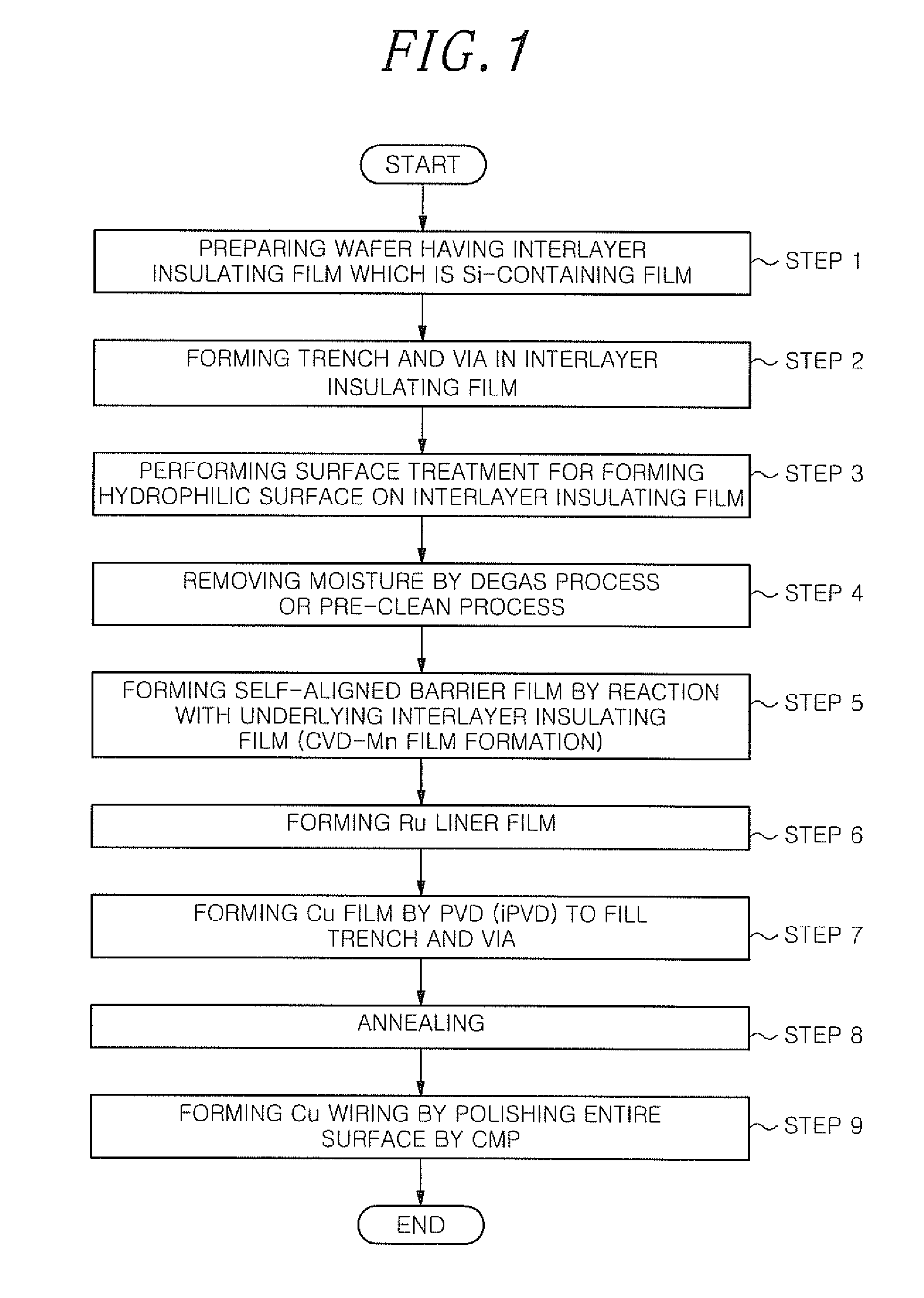
[0028]A Cu wiring forming method in accordance with an embodiment of the present invention will be described with reference to a flowchart shown in FIG. 1 and a process cross sectional view shown in FIGS. 2A to 2H.

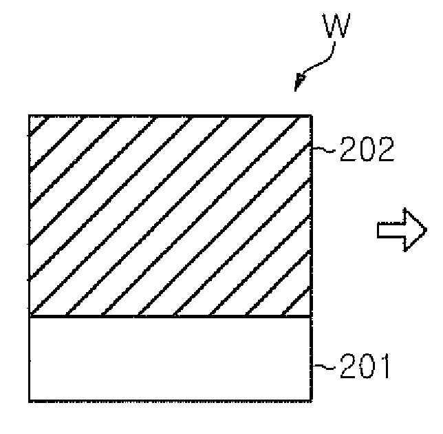
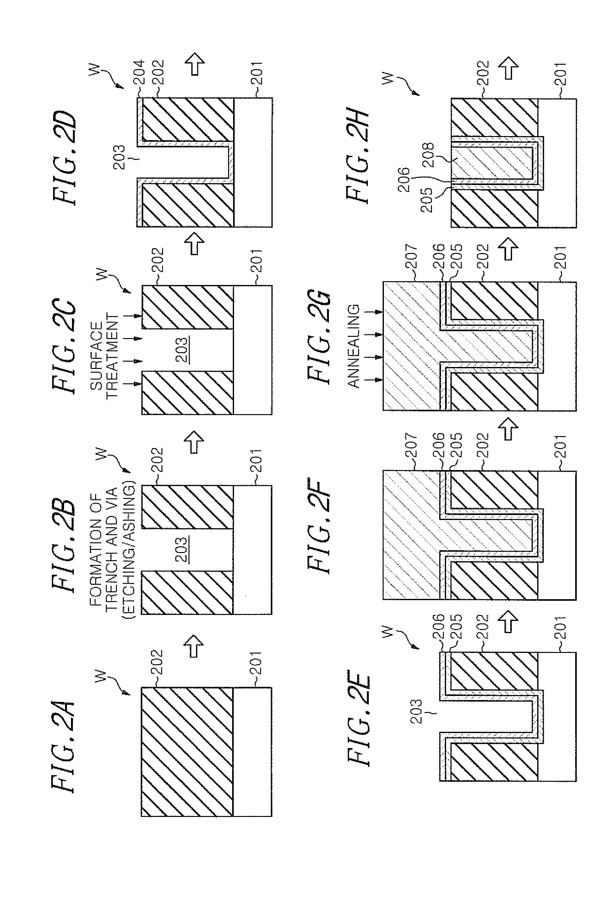
[0029]In the present embodiment, first, there is prepared a semiconductor wafer (hereinafter, simply referred to as “wafer”) W including: a base structure 201 (detailed description is omitted) including an underlying Cu wiring; and an interlayer insulating film 202 that is a Si-containing film such as a SiO2 film, a Low-k film (SiCO, SiCOH or the like) or the like formed on the base structure 201 (step 1, FIG. 2A).

[0030]Next, a trench 203 and a via (not shown) for connection to the underlying wiring are formed in a predetermined pattern by etching the interlayer insulating film, and the photoresist serving as an etch...


PUM

PropertyMeasurementUnit
thicknessaaaaaaaaaa
temperatureaaaaaaaaaa

Abstract

There is provided a Cu wiring forming method for forming a Cu wiring by filling Cu in a recess, which is formed in a predetermined pattern in a Si-containing film of a substrate. The Cu wiring forming method includes forming a Mn film, which becomes a self-aligned barrier film by reaction with an underlying base, at least on a surface of the recess by chemical vapor deposition, forming a Cu film by a physical vapor deposition to fill the recess with the Cu film, and forming a Cu wiring in the recess by polishing the entire surface of the substrate by a chemical mechanical polishing.

Description

CROSS-REFERENCE TO RELATED APPLICATIONS[0001]This application claims priority to Japanese Patent Application Nos. 2012-271020 filed on Dec. 12, 2012 and 2013-067196 filed on Mar. 27, 2013, the entire contents of which are incorporated herein by reference.FIELD OF THE INVENTION[0002]The present invention relates to a copper (Cu) wiring forming method for forming a copper wiring in a recess such as a trench or a hole formed on a substrate.BACKGROUND OF THE INVENTION[0003]Various processes such as a film formation, an etching and the like are repeatedly performed on a semiconductor wafer to manufacture a desired semiconductor device. Recently, in order to meet demands for high-speed semiconductor device, miniaturization of a wiring pattern and high level of integration, it is required to realize low resistance of wiring (high conductivity) and high electromigration resistance.[0004]Accordingly, copper (Cu) having a higher electromigration resistance and a higher conductivity (lower res...

Claims


Application Information

Patent Timeline
Patent Type & Authority Applications(United States)
IPC IPC(8): H05K3/10
CPCH05K3/107C23C14/358H01L21/02063H01L21/2855H01L21/28556H01L21/3105H01L21/76814H01L21/76826H01L21/76846H01L21/76855H01L23/53238H01L23/5329H01L2924/0002H05K1/0306H05K2201/0338
Inventor ISHIZAKA, TADAHIROSUZUKI, KENJISHIMADA, ATSUSHI
Owner TOKYO ELECTRON LTD
Why Eureka
Try Eureka