Supercharge Your Innovation With Domain-Expert AI Agents!

Methods for depositing ultra thin low resistivity tungsten film for small critical dimension contacts and interconnects

a technology of tungsten film and critical dimension, which is applied in the direction of chemical vapor deposition coating, semiconductor/solid-state device details, coatings, etc., can solve the problems of less yield, more difficulty in chemical vapor deposition of tungsten, and contact shrinkage, and achieve similar thin film resistivity, high aspect ratio features, and improved fluorine migration barriers

Active Publication Date: 2014-06-12
NOVELLUS SYSTEMS
View PDF47 Cites 24 Cited by
  • Summary
  • Abstract
  • Description
  • Claims
  • Application Information

AI Technical Summary

Benefits of technology

This approach results in improved tungsten fill with reduced resistance and enhanced barrier properties, ensuring reliable performance in advanced semiconductor devices by minimizing voids and fluorine attack, and maintaining low resistivity even at smaller dimensions.

Problems solved by technology

As semiconductor devices scale to the 32 nm technology node and beyond, shrinking contact and via dimensions make chemical vapor deposition of tungsten more challenging.
Increasing aspect ratios can lead to voids or large seams within device features, resulting in lower yields and decreased performance in microprocessor and memory chips.
Void-free fill in aggressive features like these is problematic using conventional CVD tungsten deposition techniques.

Method used


Image

  • Methods for depositing ultra thin low resistivity tungsten film for small critical dimension contacts and interconnects
  • Methods for depositing ultra thin low resistivity tungsten film for small critical dimension contacts and interconnects
  • Methods for depositing ultra thin low resistivity tungsten film for small critical dimension contacts and interconnects

Examples


Embodiment Construction

Introduction

[0025]In the following description, numerous specific details are set forth in order to provide a thorough understanding of the present invention, which pertains to forming thin tungsten films. Modifications, adaptations or variations of specific methods and structures shown and discussed herein will be apparent to those skilled in the art and are within the scope of this invention.

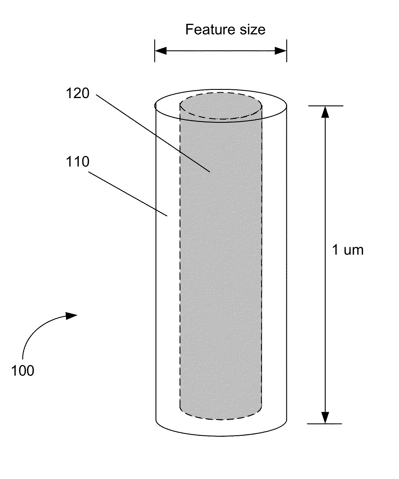
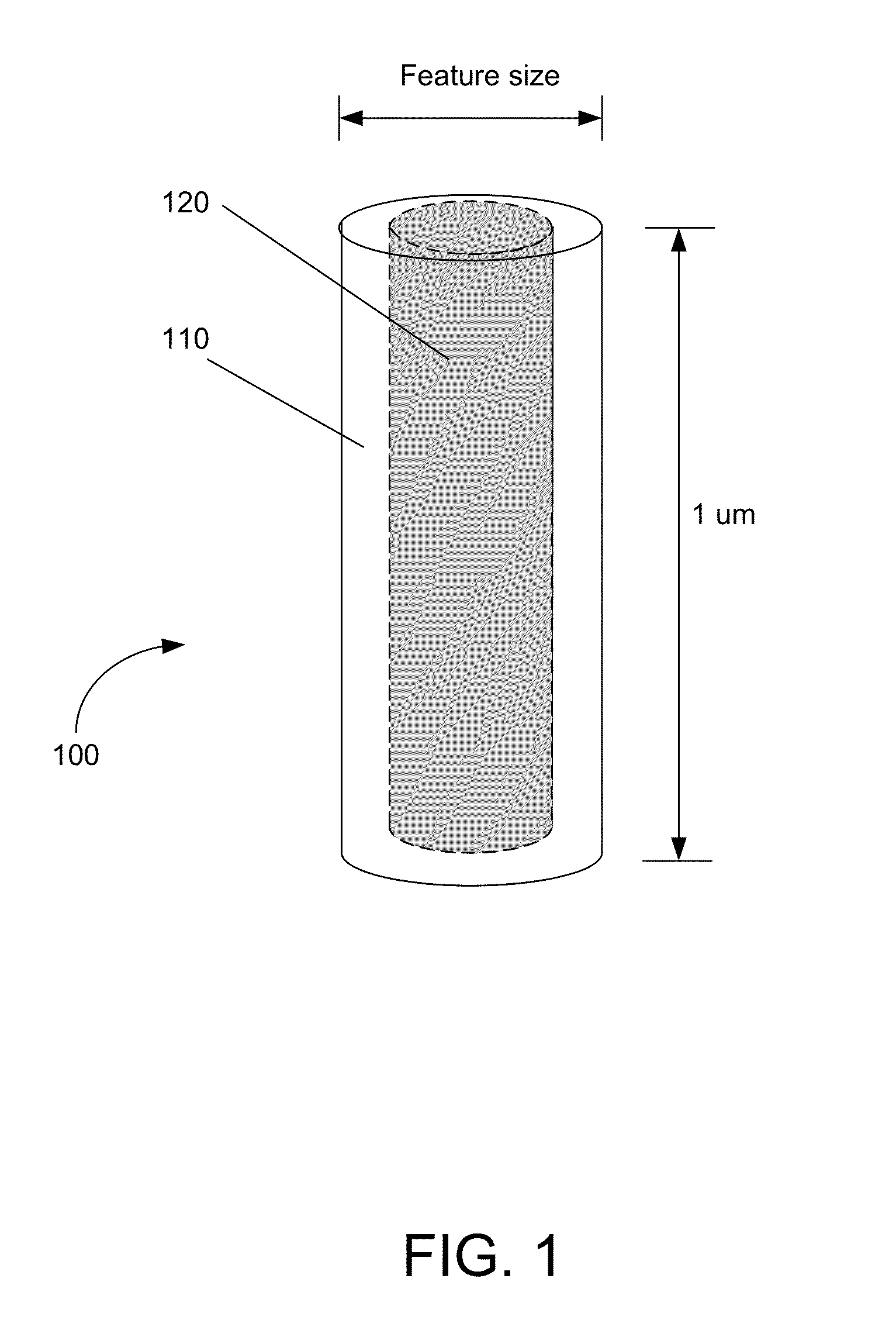
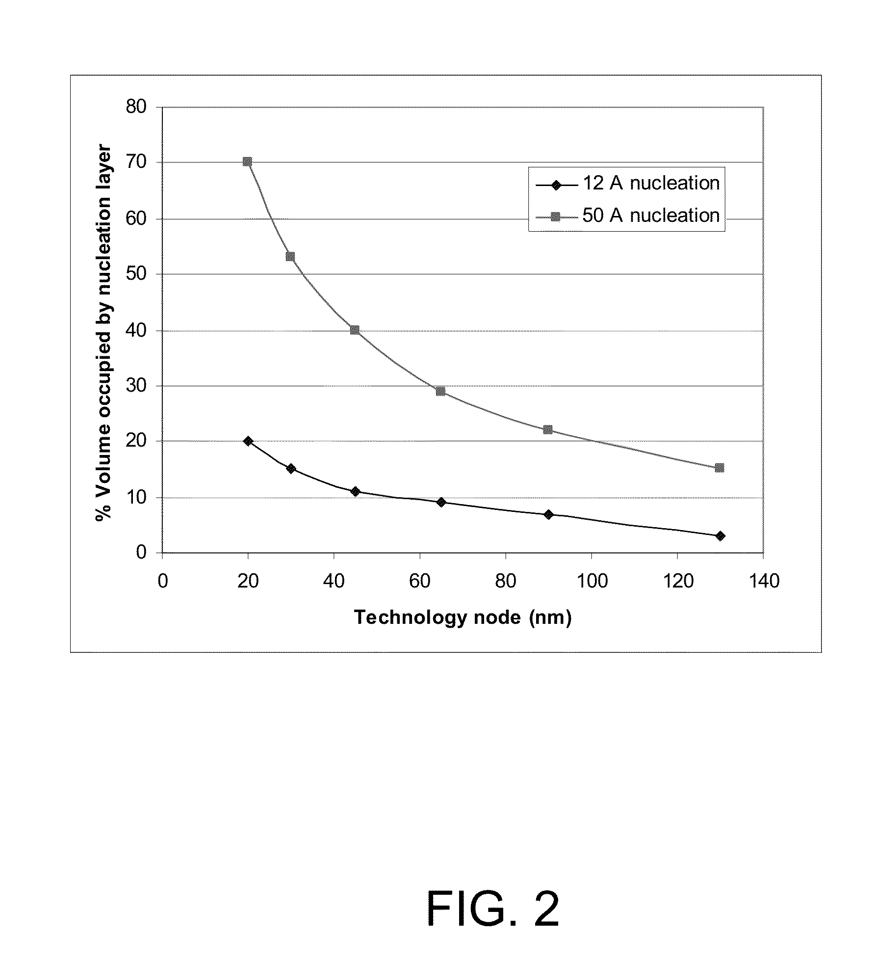
[0026]Extending tungsten to sub-32 nm technologies is critical to maintaining via / contact performance and reliability in both memory and logic devices. There are various challenges in tungsten fill as devices scale to smaller technology nodes. One challenge is preventing an increase in resistance due to the thinner films in contacts and vias. As features become smaller, the tungsten (W) contact or line resistance increases due to scattering effects in the thinner W film. While efficient tungsten deposition processes require tungsten nucleation layers, these layers typically have higher electri...


PUM

PropertyMeasurementUnit
temperatureaaaaaaaaaa
coverageaaaaaaaaaa
coverageaaaaaaaaaa

Abstract

Provided are methods of void-free tungsten fill of high aspect ratio features. According to various embodiments, the methods involve a reduced temperature chemical vapor deposition (CVD) process to fill the features with tungsten. In certain embodiments, the process temperature is maintained at less than about 350° C. during the chemical vapor deposition to fill the feature. The reduced-temperature CVD tungsten fill provides improved tungsten fill in high aspect ratio features, provides improved barriers to fluorine migration into underlying layers, while achieving similar thin film resistivity as standard CVD fill. Also provided are methods of depositing thin tungsten films having low-resistivity. According to various embodiments, the methods involve performing a reduced temperature low resistivity treatment on a deposited nucleation layer prior to depositing a tungsten bulk layer and / or depositing a bulk layer via a reduced temperature CVD process followed by a high temperature CVD process.

Description

CROSS-REFERENCE TO RELATED APPLICATIONS[0001]This application is a continuation of U.S. application Ser. No. 12 / 755,259, filed Apr. 6, 2010, titled “METHODS FOR DEPOSITING ULTRA THIN LOW RESISTIVITY TUNGSTEN FILM FOR SMALL CRITICAL DIMENSION CONTACTS AND INTERCONNECTS,” which claims the benefit under U.S.C. 119(e) to U.S. provisional application 61 / 169,954, filed Apr. 16, 2009, titled “METHOD FOR FORMING TUNGSTEN CONTACTS AND INTERCONNECTS WITH SMALL CRITICAL DIMENSIONS,” all of which are incorporated herein in their entireties for all purposes.BACKGROUND[0002]The deposition of tungsten films using chemical vapor deposition (CVD) techniques is an integral part of many semiconductor fabrication processes. Tungsten films may be used as low resistivity electrical connections in the form of horizontal interconnects, vias between adjacent metal layers, and contacts between a first metal layer and the devices on the silicon substrate. In a conventional tungsten deposition process, the waf...

Claims


Application Information

Patent Timeline
Patent Type & Authority Applications(United States)
IPC IPC(8): H01L21/768H01L21/67
CPCH01L21/76879H01L21/76843H01L21/67017C23C16/0272C23C16/045C23C16/14C23C16/45523H01L21/28556H01L21/76876H01L21/76877H01L2924/0002H01L2924/00C23C16/52H01L21/76816H01L21/76895H01L23/53266H01L23/535
Inventor CHEN, FENGHUMAYUN, RAASHINADANEK, MICHALCHANDRASHEKAR, ANAND
Owner NOVELLUS SYSTEMS
Features
  • R&D
  • Intellectual Property
  • Life Sciences
  • Materials
  • Tech Scout
  • Unparalleled Data Quality
  • Higher Quality Content
  • 60% Fewer Hallucinations
Learn More