Graphene structure, graphene device including same, and method of manufacturing graphene structure

a graphene and graphene technology, applied in the direction of graphene, nano-carbon, semiconductor devices, etc., can solve the problems of non-uniform distribution of silicon and carbon, affecting the uniformity of graphene layers, and reducing electron mobility accordingly

Active Publication Date: 2014-06-26
SAMSUNG ELECTRONICS CO LTD
View PDF9 Cites 25 Cited by
  • Summary
  • Abstract
  • Description
  • Claims
  • Application Information

AI Technical Summary

Benefits of technology

[0021]The metal-silicide may be formed over a region of the silicon carbide substrate containing more silicon than carbon on a surface of the silicon carbide substr...

Problems solved by technology

However, it has limitations in terms of forming a uniform graphene layer and thus electron mobility also decreases accordingly.
Si...

Method used


Image

  • Graphene structure, graphene device including same, and method of manufacturing graphene structure
  • Graphene structure, graphene device including same, and method of manufacturing graphene structure
  • Graphene structure, graphene device including same, and method of manufacturing graphene structure

Examples


Embodiment Construction

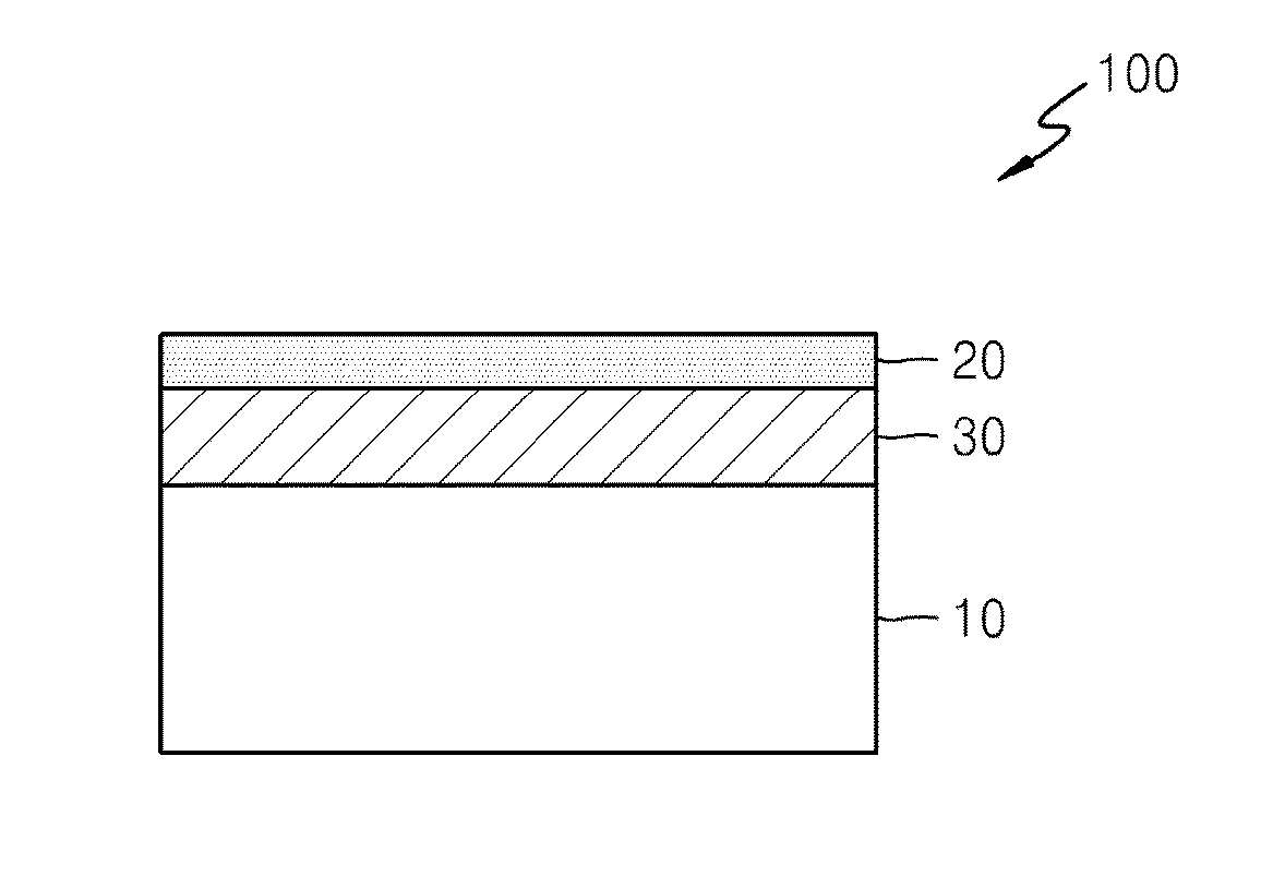
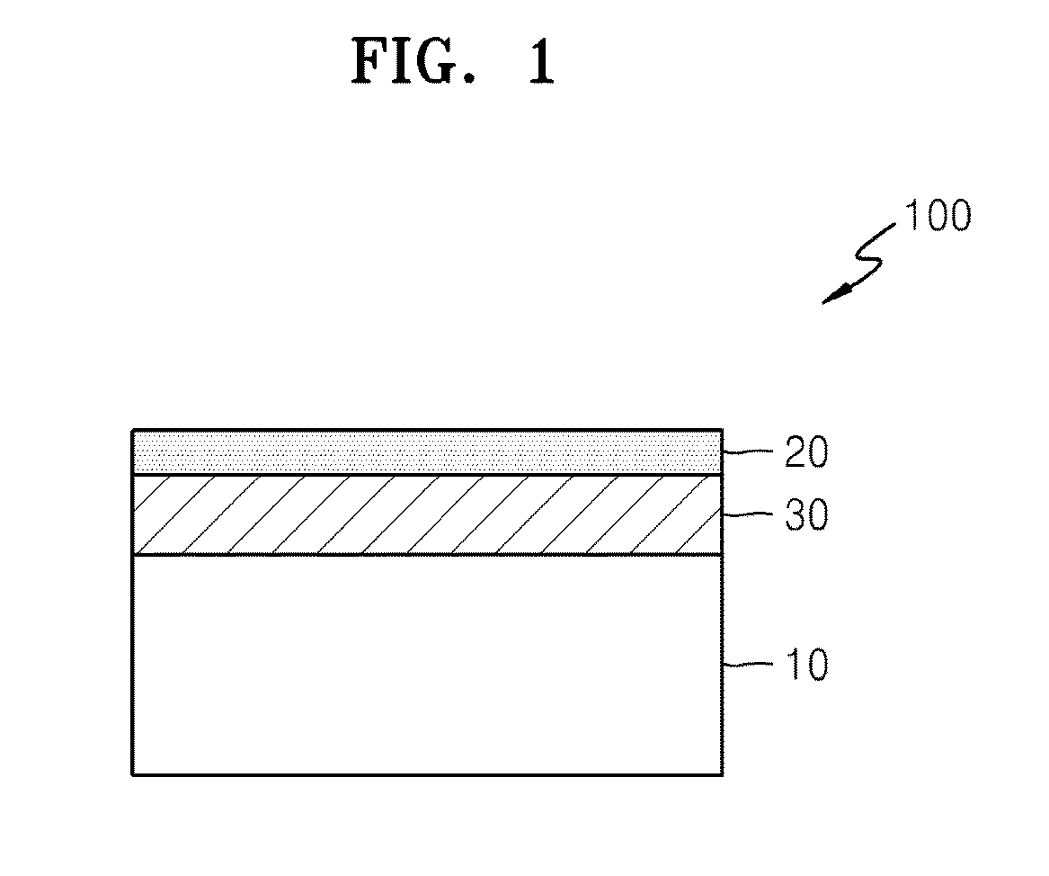
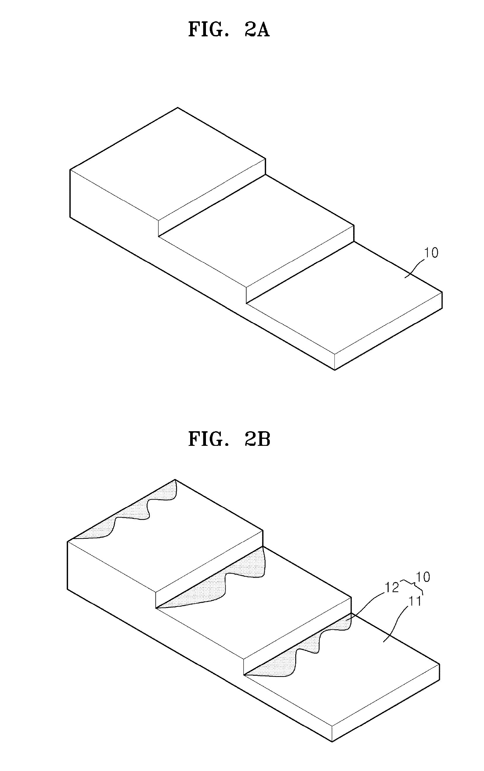
[0052]Reference will now be made in detail to example embodiments, examples of which are illustrated in the accompanying drawings, wherein like reference numerals refer to like elements throughout. In this regard, the present example embodiments may have different forms and should not be construed as being limited to the descriptions set forth herein. Specific structural and functional details disclosed herein are merely representative for purposes of describing example embodiments, and thus may be embodied in many alternate forms and should not be construed as limited to only example embodiments set forth herein. Therefore, it should be understood that there is no intent to limit example embodiments to the particular forms disclosed, but on the contrary, example embodiments are to cover all modifications, equivalents, and alternatives falling within the scope of the disclosure.

[0053]In the drawings, the thicknesses of layers and regions may be exaggerated for clarity, and like numb...


PUM


Abstract

A method of manufacturing a graphene structure, the graphene structure, and a graphene device including the graphene structure, include depositing a metal layer over a silicon carbide substrate; and performing, at a first temperature, a heat treatment on the silicon carbide substrate over which the metal layer is deposited to form a composite layer and a graphene layer on the silicon carbide substrate. The composite layer includes a metal.

Description

CROSS-REFERENCE TO RELATED APPLICATIONS[0001]This application claims the benefit of priority from Korean Patent Application No. 10-2012-0151337, filed on Dec. 21, 2012 in the Korean Intellectual Property Office, the disclosure of which is incorporated herein by reference in its entirety.BACKGROUND[0002]1. Field[0003]The present disclosure relates to a graphene structure, a graphene device including the same, and a method of manufacturing the graphene structure.[0004]2. Description of the Related Art[0005]In general, graphite has a structure in which plate-shaped 2D graphenes that are formed by hexagonally connected carbon atoms are stacked.[0006]The graphene may be usefully used for various electrical devices such as display device electrodes or solar cell electrodes because of its excellent transparency and conductivity.[0007]The graphene is formed through a thermal treatment process after supplying a carbon supply source to a metal catalyst and subsequently, obtained graphene is s...

Claims


Application Information

Patent Timeline
IPC IPC(8): H01L21/283H01L29/43
CPCH01L21/02378H01L21/0243H01L21/02491H01L21/02494H01L21/283H01L21/02612H01L29/45H01L29/1606H01L29/1608H01L21/02527H01L29/78684C01B32/184H01L29/66742B01J6/00C23C16/06C01B2204/22C01B2204/02
Inventor AHN, JOUNG-REALSHIN, HA-CHULSONG, IN-KYUNG
Owner SAMSUNG ELECTRONICS CO LTD
Why Eureka
Try Eureka