Liquid crystal display device and manufacturing method of liquid crystal display device
a liquid crystal display and manufacturing method technology, applied in optics, instruments, electrical equipment, etc., can solve the problems of flicker, fluctuation of luminance, and potential of pixel electrodes, and achieve the effect of reducing flicker and reliably suppressing the crosstalk between pixel electrodes and source lines
- Summary
- Abstract
- Description
- Claims
- Application Information
AI Technical Summary
Benefits of technology
Problems solved by technology
Method used
Image

Examples
first embodiment
[0051](Configuration of LCD Device)
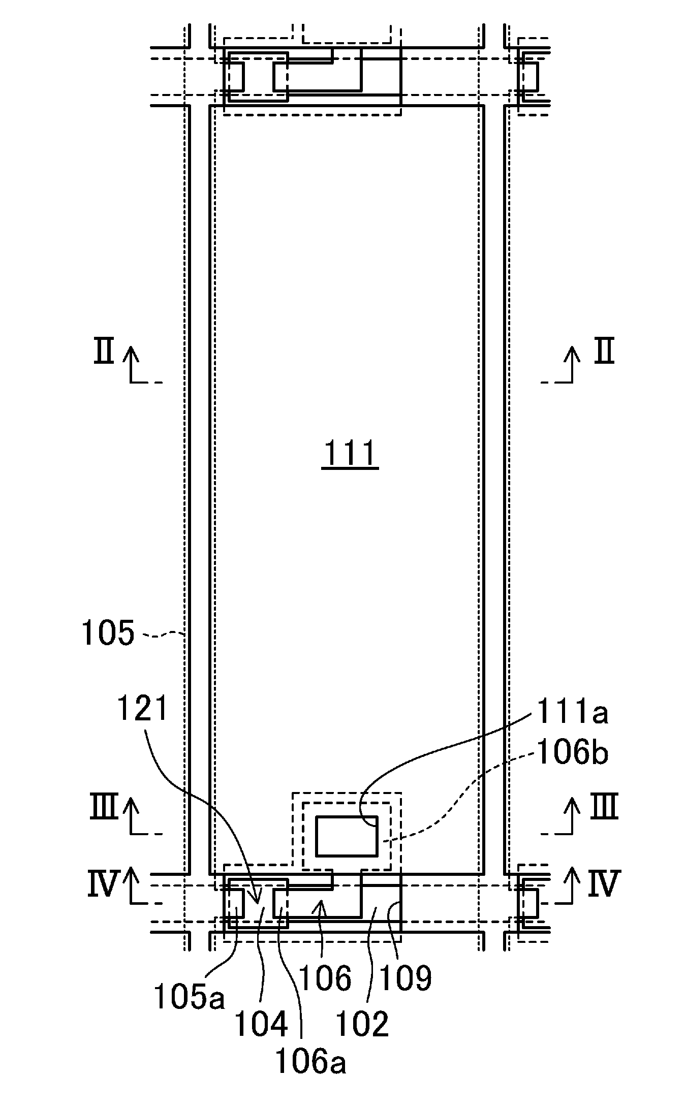
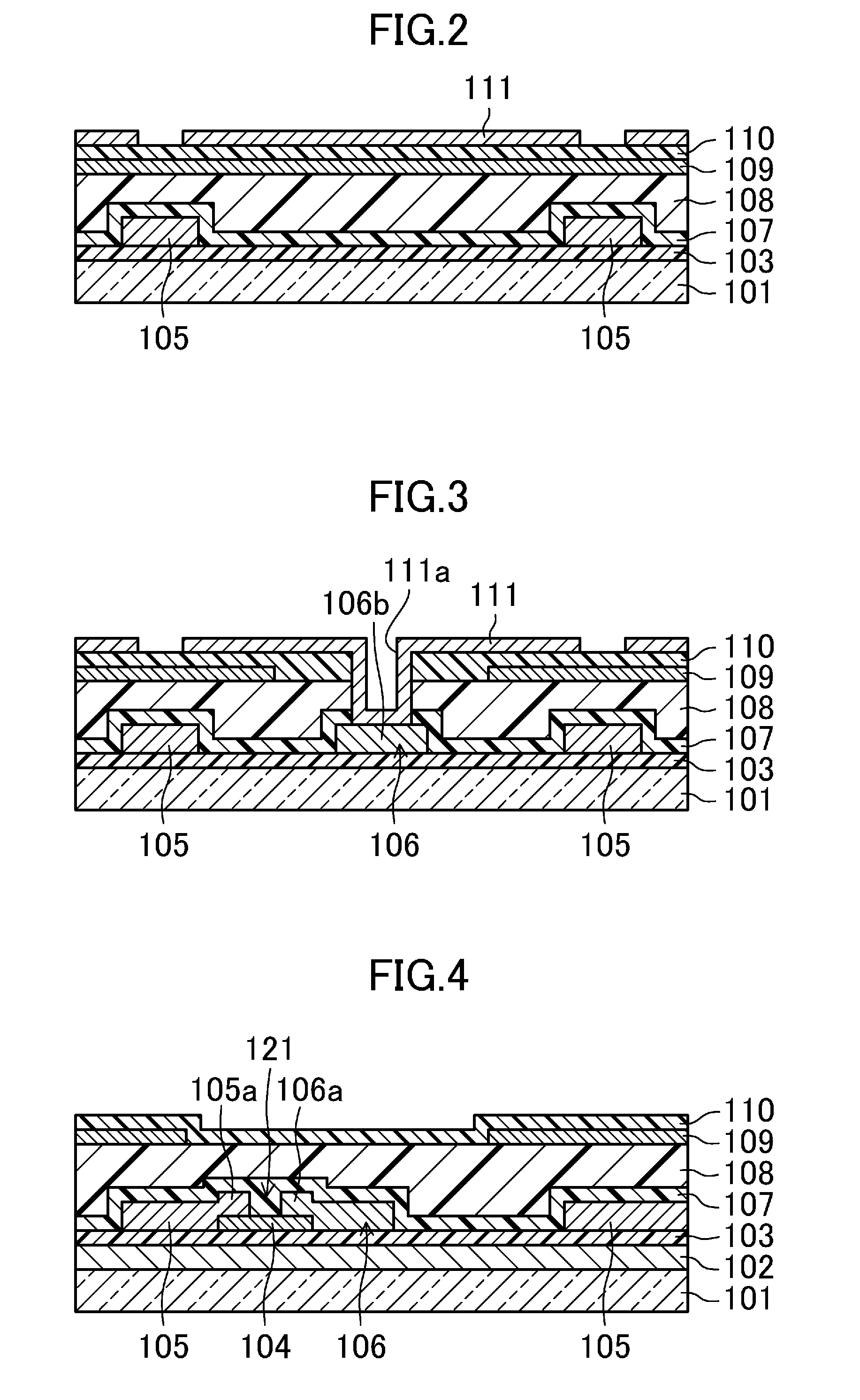
[0052]As shown in, e.g., FIGS. 1 to 4, an array substrate that together with a counter substrate forms an LCD device with a liquid crystal material enclosed therebetween includes: a transparent substrate 101; a plurality of gate lines 102 provided on the transparent substrate 101 so as to extend parallel to each other; a gate insulating film 103 provided so as to cover the gate lines 102; a plurality of source lines 105 provided on the gate insulating film 103 so as to extend parallel to each other in a direction perpendicular to the gate lines 102; oxide semiconductor layers 104 provided in an island shape on the gate insulating film 103 so as to correspond to each intersection of the gate line 102 and the source line 105, namely each sub-pixel, and each provided so as to overlap a part of a corresponding one of the gate lines 102; drain lines 106 each provided so that its one end overlaps a part of a corresponding one of the oxide semiconductor l...
second embodiment
[0080]The pixel electrode 111 has a continuous shape in the pixel region in the first embodiment (FIG. 1). However, the pixel electrode 111 is not limited to this, and may have, e.g., a shape having an opening such as a plurality of slits 111b as shown in FIGS. 9 and 10. Specifically, even if an LCD device having a display mode with excellent viewing angle characteristics, such as an in plane switching (IPS) mode or an advanced fringe field switching (AFFS) mode, is produced by using such a pixel electrode 111, parasitic capacitance between the pixel electrode 111 and the source line 105 is similarly reduced, and crosstalk between the pixel electrode 111 and the source line 105 is reliably suppressed, whereby flicker can be reduced.
third embodiment
[0081]The transparent auxiliary capacitor electrode 109 need only be provided in a sufficiently large area including the region where the source line 105 overlaps the pixel electrode 111 and the vicinity thereof. For example, the transparent auxiliary capacitor electrode 109 may have an opening 109a with a rectangular shape as shown in FIGS. 11 and 12 or other shapes so that auxiliary capacitance does not become too large. That is, even if the opening 109a is formed at a position located sufficiently away from the source line 105, crosstalk between the pixel electrode 111 and the source line 105 can be reliably suppressed and flicker can be reduced as long as a sufficient shielding effect of the transparent auxiliary capacitor electrode 109 is obtained near the source line 105.
PUM
| Property | Measurement | Unit |
|---|---|---|
| capacitance | aaaaa | aaaaa |
| transparent | aaaaa | aaaaa |
| voltage | aaaaa | aaaaa |
Abstract
Description
Claims
Application Information
 - Generate Ideas
- Intellectual Property
- Life Sciences
- Materials
- Tech Scout
- Unparalleled Data Quality
- Higher Quality Content
- 60% Fewer Hallucinations
Browse by: Latest US Patents, China's latest patents, Technical Efficacy Thesaurus, Application Domain, Technology Topic, Popular Technical Reports.
© 2025 PatSnap. All rights reserved.Legal|Privacy policy|Modern Slavery Act Transparency Statement|Sitemap|About US| Contact US: help@patsnap.com