This helps you quickly interpret patents by identifying the three key elements:
Problems solved by technology
Method used
Benefits of technology
Benefits of technology
The present invention aims to solve problems in the conventional wiring bonding of semiconductor chips to insulating base materials. The invention provides a wiring that can withstand resin seal material during the packaging process and has greater adhesive strength to the structure in which it is provided, reducing problems such as wire falling, dislocation, and disconnection.
Problems solved by technology
Thus, the seal material containing large amounts of inorganic filling material as described above has extremely inferior fluidity.
In such case, considerably external force is applied to the wire used for the bonding, and there was a problem in that the reliability of the semiconductor device would be impaired due to the breakage or damage of the wire.
Nevertheless, expensive gold is often used as the wire.
Thus, increasing the wire diameter means increased costs.
In addition, with the wire bonding method, since the wire spacing cannot be narrowed in consideration of the sweep amount of the wire, there is a problem in that the wiring density is low.
Method used
Image
Click on the blue label to locate the original text in one second.
Reading with bidirectional positioning of images and text.
Examples
first embodiment
[0039]The preferred embodiments of the method of mounting a semiconductor chip according to the present invention are now explained with reference to the drawings.
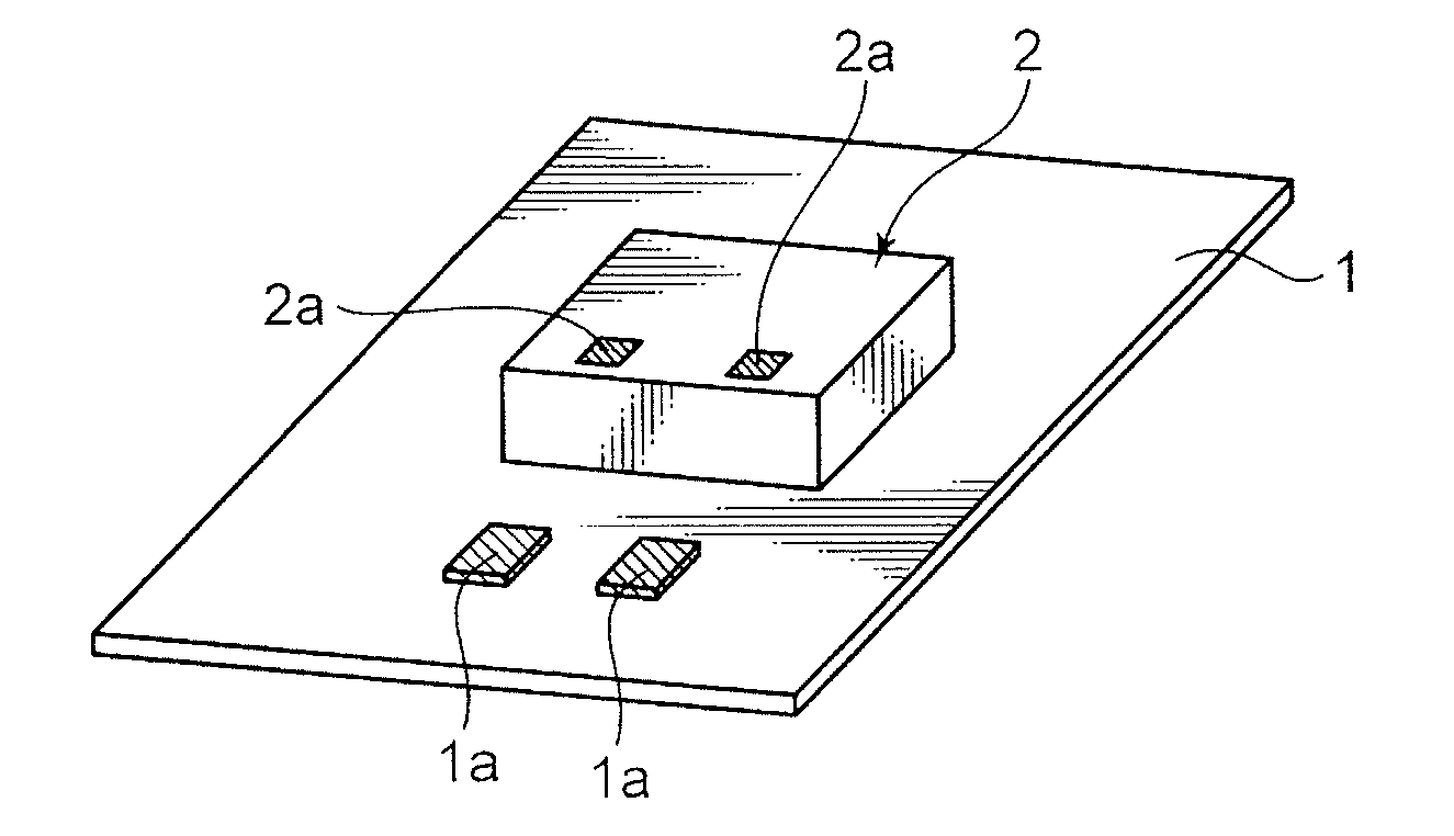
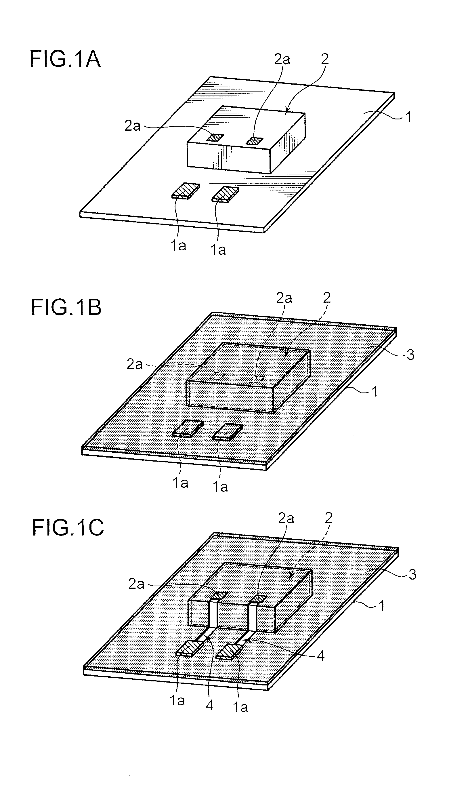
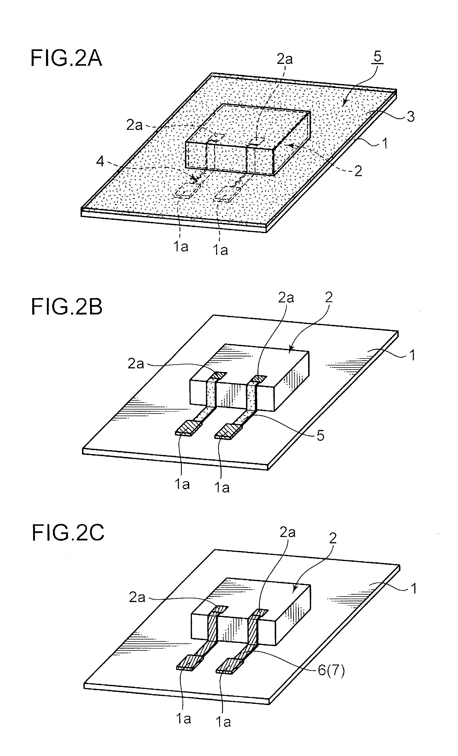
[0040]FIG. 1 and FIG. 2 are schematic diagrams explaining the respective processes in the method of mounting a semiconductor chip of this embodiment. Note that, in FIG. 1 and FIG. 2, 1 represents an insulating base material, 1a represents an electrode pad, 2 represents a semiconductor chip, 2a represents a bonding pad, 3 represents a resin coating, 4 represents a wiring gutter, 5 represents a plating catalyst, 6 represents an electroless platingcoating, and 7 represents a wiring.
[0041]In the production method of this embodiment, as shown in FIG. 1A, foremost, an insulating base material 1 mounted with a semiconductor chip 2 in a predetermined chip mounting area is prepared.
[0042]Note that the semiconductor chip 2 is fixed to the predetermined chip mounting area on the surface of the insulating base material 1 using an adh...
second embodiment
[0101]A preferred method of connecting a plurality of semiconductor chips according to the present invention is now explained with reference to the drawings. Note that, since the respective processes are the same as the processes explained in the first embodiment, the detailed explanation of redundant portions is omitted. Moreover, since the components given the same reference numerals as the reference numerals of the first embodiment are the same components, the explanation thereof is omitted.
[0102]FIG. 4 and FIG. 5 are schematic diagrams explaining the respective processes in the method of connecting a plurality of semiconductor chips of this embodiment. In FIG. 4 and FIG. 5, 1 represents an insulating base material, 2 represents a first semiconductor chip, 12 represents a second semiconductor chip, 2a, 12a represent bonding pads, 3 represents a resin coating, 4 represents a wiring gutter, 5 represents a plating catalyst, and 6 represents an electroless platingcoating.
[0103]In th...
embodiment
Third (2) Embodiment
[0147]Another embodiment of the three-dimensional structure 200 is a three-dimensional structure that has a concave-convex form including a gutter for wiring having at least partially a width of 20 μm or less, wherein at least a part of a wiring conductor is embedded in the gutter for wiring, and a wiring that extends in such a manner as to creep along the concave-convex form is provided.
[0148]FIGS. 23 and 24 are schematic diagrams explaining the three-dimensional structure 200 of the present embodiment. Note that, in FIGS. 23 and 24, reference numeral 901 represents an insulating base material, 901a an electrode pad, 902 a semiconductor chip, 902a a pad part, 905 a gutter for wiring, and 907 a wiring (wiring conductor).
[0149]As illustrated in FIG. 23, in the three-dimensional structure of the present embodiment the gutter for wiring 905 is provided on the surface of the insulating base material 901 and the surface of the semiconductor chip 902. Thus, the surface...
PUM
Abstract
One aspect of the present invention is a three-dimensional structure that has a concave-convex form including a gutter for wiring having at least partially a width of 20 μm or less, wherein at least a part of a wiring conductor is embedded in the gutter for wiring, and a wiring that extends in such a manner as to creep along the concave-convex form is provided.
Description
TECHNICAL FIELD[0001]The present invention mainly relates to a three-dimensional structure for wiring formation.BACKGROUND ART[0002]Conventionally, a semiconductor device in which a semiconductorchip is mounted on an insulating base material is well known. As the method of mounting a semiconductorchip on an insulating base material and electrically connecting the semiconductor chip to an electrode pad formed on the insulating base material surface, the wire bonding method is widely used.[0003]The wire connection method based on wire bonding is a method, as shown in FIG. 6, of mutually connecting a bonding pad 22a formed on an upper surface of a semiconductor chip 22 and an electrode pad 11a on the side of an insulating base material 11 via a wire 13 formed from gold, copper or the like and having a diameter of several 10 μm. More specifically, this is a method of connecting a wire protruding from the tip of a capillary through a throughhole formed at the center of a movable capill...
Claims
Application Information
Patent Timeline
Application Date:The date an application was filed.
Publication Date:The date a patent or application was officially published.
First Publication Date:The earliest publication date of a patent with the same application number.
Issue Date:Publication date of the patent grant document.
PCT Entry Date:The Entry date of PCT National Phase.
Estimated Expiry Date:The statutory expiry date of a patent right according to the Patent Law, and it is the longest term of protection that the patent right can achieve without the termination of the patent right due to other reasons(Term extension factor has been taken into account ).
Invalid Date:Actual expiry date is based on effective date or publication date of legal transaction data of invalid patent.

